32 BIT ADDER FOR LOW VOLTAGE OPERATION WITH

32 -BIT ADDER FOR LOW VOLTAGE OPERATION WITH LEVEL CONVERTERS PRIYADHARSHINI S
2 OBJECTIVES • To reduce power consumption in a 32 -bit adder circuit by reducing the voltage of operation • To study the effect of voltage reduction on the delay of the circuit • To identify an optimal voltage of operation at which the power-delay product is low • To design a level converter to make the circuit compatible with other circuits
3 TOOLS USED • Model. Sim: To verify the functionality of the circuit • Leonardo Spectrum: To synthesize the verilog gate level netlist • MATLAB: To synthesize the netlist compatible with Power. Sim • Design Architect: To obtain the transistor level design of gates • LTSpice: To evaluate the delays of individual gates • Power. Sim: To assess the performance of the circuit at different voltages
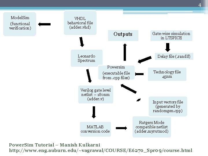
4 Model. Sim (functional verification) VHDL behavioral file (adder. vhd) Outputs Leonardo Spectrum Gate-wise simulation in LTSPICE Delay file (. randlf) Powersim (executable file from. cpp files) Verilog gate level netlist – 180 nm (adder. v) MATLAB conversion code Technology file 45 nm Input vectors file (generated by randomgen. cpp) Rutgers Mode compatible netlist (adder. myrutmod) Power. Sim Tutorial – Manish Kulkarni http: //www. eng. auburn. edu/~vagrawal/COURSE/E 6270_Spr 09/course. html
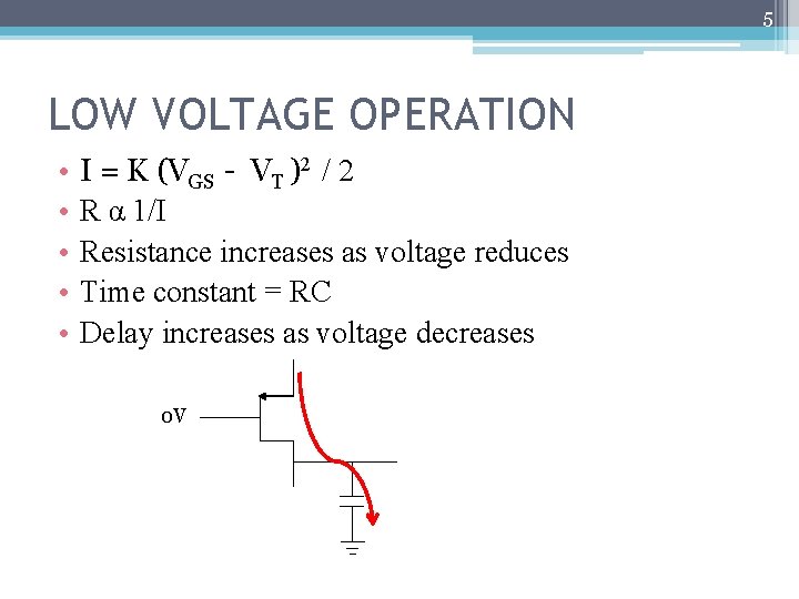
5 LOW VOLTAGE OPERATION • • • I = K (VGS - VT )2 / 2 R α 1/I Resistance increases as voltage reduces Time constant = RC Delay increases as voltage decreases 0 V
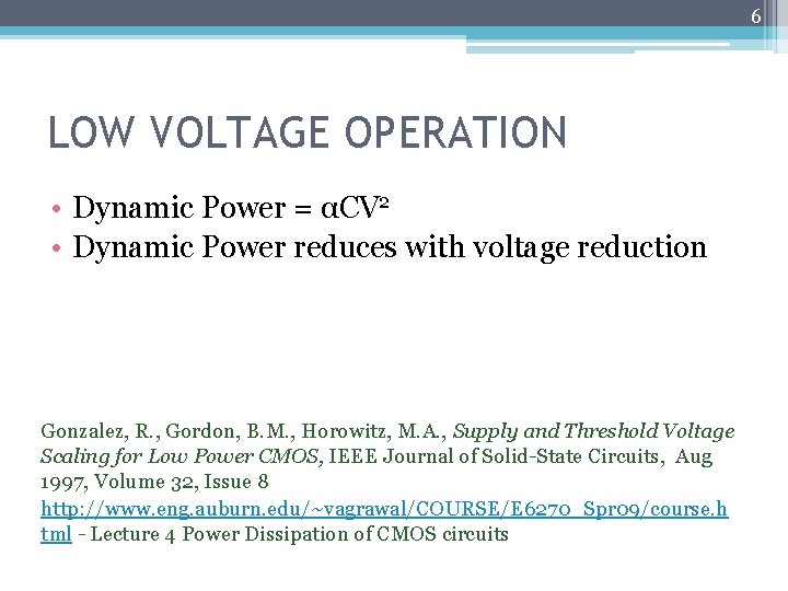
6 LOW VOLTAGE OPERATION • Dynamic Power = αCV 2 • Dynamic Power reduces with voltage reduction Gonzalez, R. , Gordon, B. M. , Horowitz, M. A. , Supply and Threshold Voltage Scaling for Low Power CMOS, IEEE Journal of Solid-State Circuits, Aug 1997, Volume 32, Issue 8 http: //www. eng. auburn. edu/~vagrawal/COURSE/E 6270_Spr 09/course. h tml - Lecture 4 Power Dissipation of CMOS circuits
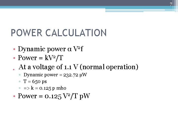
7 POWER CALCULATION • Dynamic power α V 2 f • Power = k. V 2/T • At a voltage of 1. 1 V (normal operation) ▫ Dynamic power = 232. 72 µW ▫ T = 650 ps ▫ => k = 0. 125 p mho • Power = 0. 125 V 2/T p. W
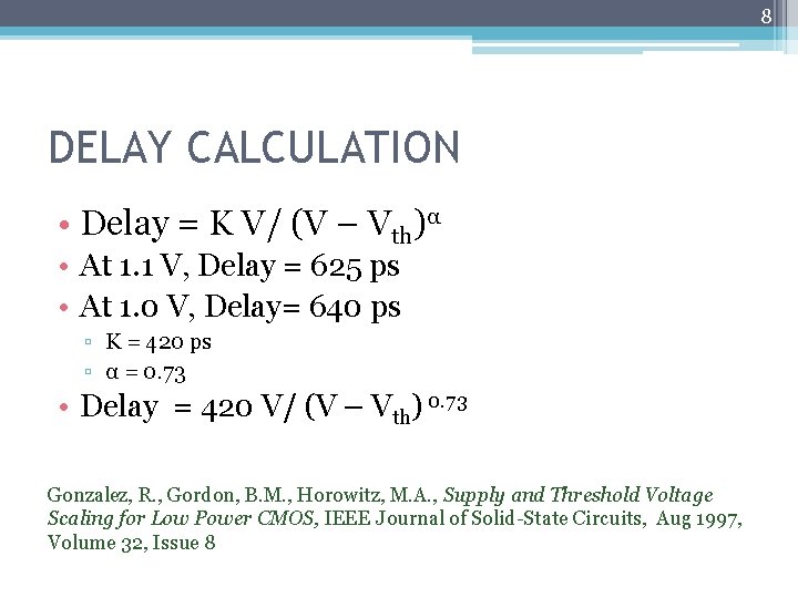
8 DELAY CALCULATION • Delay = K V/ (V – Vth)α • At 1. 1 V, Delay = 625 ps • At 1. 0 V, Delay= 640 ps ▫ K = 420 ps ▫ α = 0. 73 • Delay = 420 V/ (V – Vth) 0. 73 Gonzalez, R. , Gordon, B. M. , Horowitz, M. A. , Supply and Threshold Voltage Scaling for Low Power CMOS, IEEE Journal of Solid-State Circuits, Aug 1997, Volume 32, Issue 8
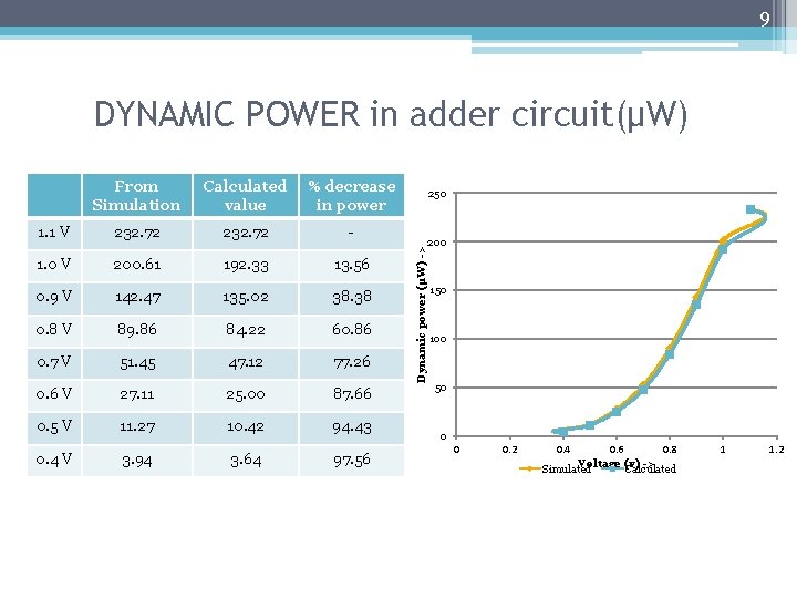
9 DYNAMIC POWER in adder circuit(µW) Calculated value % decrease in power 1. 1 V 232. 72 - 1. 0 V 200. 61 192. 33 13. 56 0. 9 V 142. 47 135. 02 38. 38 0. 8 V 89. 86 84. 22 60. 86 0. 7 V 51. 45 47. 12 77. 26 0. 6 V 27. 11 25. 00 87. 66 0. 5 V 11. 27 10. 42 94. 43 0. 4 V 3. 94 3. 64 97. 56 250 Dynamic power (µW) -> From Simulation 200 150 100 50 0 0 0. 2 0. 4 0. 6 0. 8 Voltage (v) -> Simulated Calculated 1 1. 2
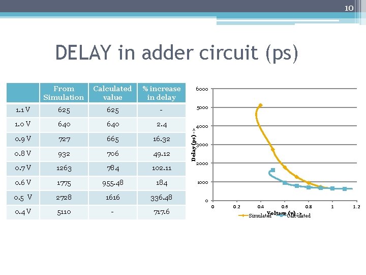
10 DELAY in adder circuit (ps) Calculated value % increase in delay 6000 1. 1 V 625 - 5000 1. 0 V 640 2. 4 4000 0. 9 V 727 665 16. 32 0. 8 V 932 706 49. 12 0. 7 V 1263 784 102. 11 0. 6 V 1775 955. 48 184 0. 5 V 2728 1616 336. 48 0. 4 V 5110 - 717. 6 Delay (ps) -> From Simulation 3000 2000 1000 0 0 0. 2 0. 4 0. 6 0. 8 Voltage (v) -> Simulated Calculated 1 1. 2
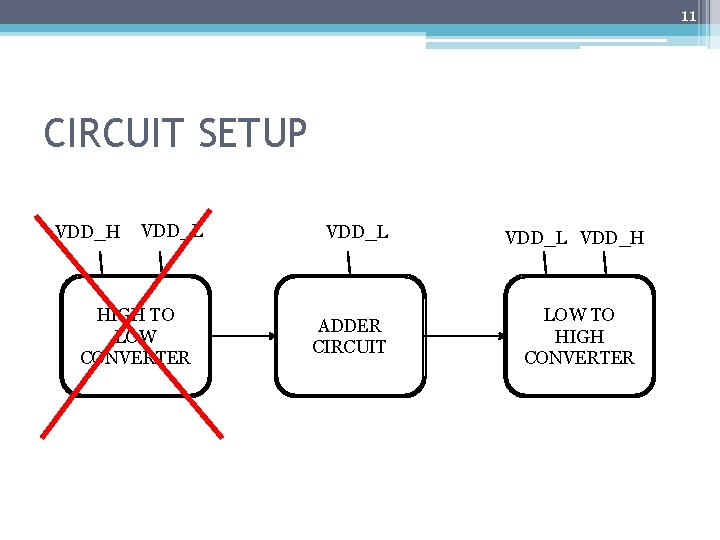
11 CIRCUIT SETUP VDD_H VDD_L HIGH TO LOW CONVERTER VDD_L ADDER CIRCUIT VDD_L VDD_H LOW TO HIGH CONVERTER
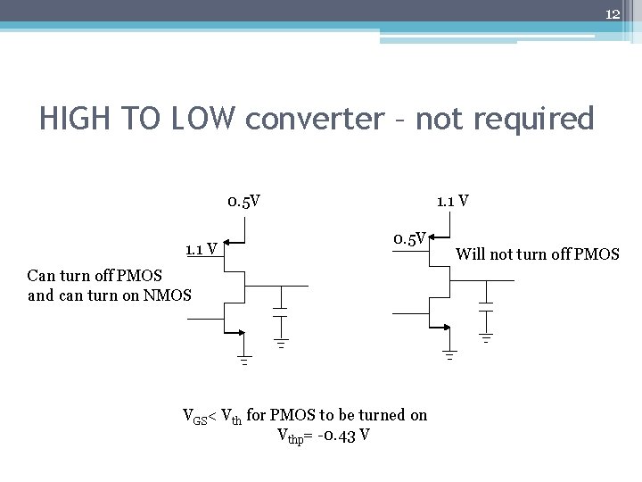
12 HIGH TO LOW converter – not required 0. 5 V 1. 1 V 0. 5 V Can turn off PMOS and can turn on NMOS VGS< Vth for PMOS to be turned on Vthp= -0. 43 V Will not turn off PMOS
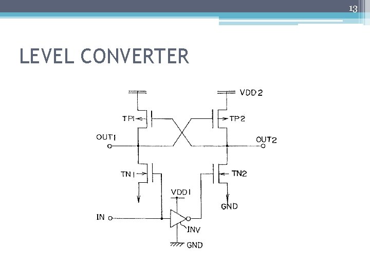
13 LEVEL CONVERTER
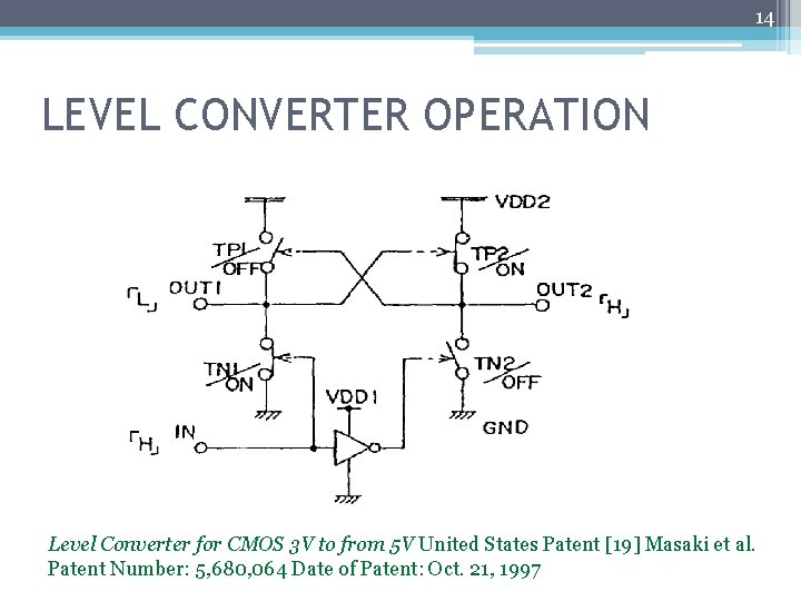
14 LEVEL CONVERTER OPERATION Level Converter for CMOS 3 V to from 5 V United States Patent [19] Masaki et al. Patent Number: 5, 680, 064 Date of Patent: Oct. 21, 1997
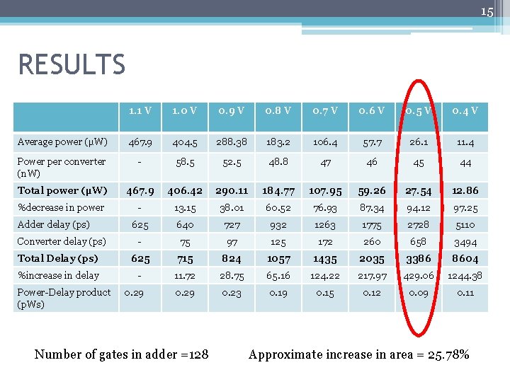
15 RESULTS 1. 1 V 1. 0 V 0. 9 V 0. 8 V 0. 7 V 0. 6 V 0. 5 V 0. 4 V Average power (µW) 467. 9 404. 5 288. 38 183. 2 106. 4 57. 7 26. 1 11. 4 Power per converter (n. W) - 58. 5 52. 5 48. 8 47 46 45 44 Total power (µW) 467. 9 406. 42 290. 11 184. 77 107. 95 59. 26 27. 54 12. 86 %decrease in power - 13. 15 38. 01 60. 52 76. 93 87. 34 94. 12 97. 25 640 727 932 1263 1775 2728 5110 - 75 97 125 172 260 658 3494 Total Delay (ps) 625 715 824 1057 1435 2035 3386 8604 %increase in delay - 11. 72 28. 75 65. 16 124. 22 217. 97 429. 06 1244. 38 0. 29 0. 23 0. 19 0. 15 0. 12 0. 09 0. 11 Adder delay (ps) Converter delay (ps) Power-Delay product (p. Ws) Number of gates in adder =128 Approximate increase in area = 25. 78%
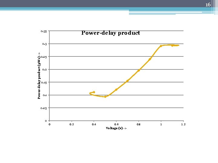
16 0. 35 Power-delay product (p. Ws) -> 0. 3 0. 25 0. 2 0. 15 0. 1 0. 05 0 0 0. 2 0. 4 0. 6 Voltage (v) -> 0. 8 1 1. 2
17 CONCLUSION • The adder circuit can be operated at 0. 5 V in order to minimize power • Parameters other than power-delay product should be considered to decide on the operating voltage
18 FUTURE WORK • Evaluating performance of circuit with a few chains of gates operating at low voltages • Lowering power by introducing low-threshold transistors in non-critical paths
19 REFERENCES • Gonzalez, R. , Gordon, B. M. , Horowitz, M. A. , Supply and Threshold Voltage Scaling for Low Power CMOS, IEEE Journal of Solid-State Circuits, Aug 1997, Volume 32, Issue 8 • Anantha P. Chandrakasan, Samuel Sheng, Robert W. Brodersen, Low. Power CMOS Digital Design, IEEE Journal of Solid-State Circuits, Volume 27, No. 4, April 1992 • Masaki et al. , Level Converter for CMOS 3 V to from 5 V, United States Patent [19] Patent Number: 5, 680, 064 Date of Patent: Oct. 21, 1997 • Kiat-Seng Yeo, Kaushik Roy, Low-Voltage, Low-Power VLSI Subsystems, Mc. Graw Hill • Class lectures

20 THANK YOU
- Slides: 20