3 D IC RELIABILITY Xinxin Yu Hao Wu

3 D IC RELIABILITY Xinxin Yu, Hao Wu

Packaging Technology Evolution

3 D IC
 IC Success")
Requirements for 3 D (TSV) IC Success
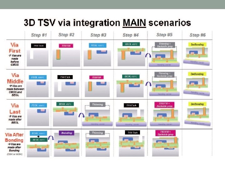
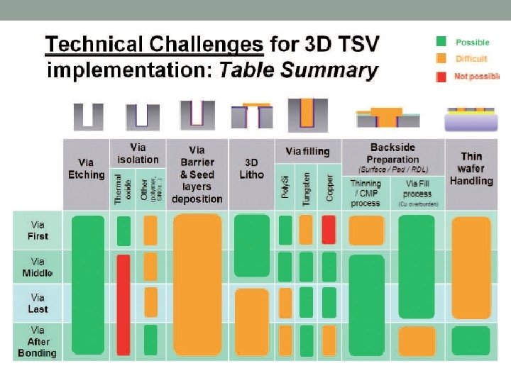
 IC Design Flow Vision")
3 D (TSV) IC Design Flow Vision

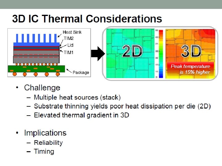
Reliability Issues • Common Design • Electromigration • Self-heating • Hot carriers • Latchup • Overvoltage failure • 3 D IC • Stress

3 D Model Construction for Thermal and stress ANSYS

Thermal Equation

Parameters

Boundary Condition

Simulation results from Cadence

Current and voltage inputs

Application of Submodeling

Temperature Distribution

CTM-based thermal analyzer • Chip Thermal Mode • CTMs are first generated for all the chips in 3 D IC or Si. P. • The thermal analyzer then simulates and updates temperature on each of the chips • Continue looking up in CTMs for updated power maps and recalculate temperatures, until the total power on each chip converged • Detailed full chip sub-models are then constructed from the metal layer distributions in CTM and physical chip geometry

Power density map

TSV Induced Stress and Reliability

3 D IC Stress Reliability

Single TSV with various structural configurations • Due to thermal expansion mismatch between constituent materials, the fabrication of TSVs can induce thermal stresses to degrade the performance of stress sensitive devices. Thermo-Mechanical Reliability of 3 -D ICs containing Through Silicon Vias Kuan H. Lu, Xuefeng Zhang, Suk-Kyu Ryu*, Jay Im, Rui Huang*, and Paul S. Ho, 2009 Electronic Components and Technology Conference

Two-by-two copper TSV array • the methodology will be extended to analyze the stress interaction in TSV arrays

Analytical Plane Strain Approximation • When two TSVs are aligned along the y- direction, the normal stress is intensified and the shear stress is suppressed in the space • In contrast, the normal stress is suppressed and the shear stress is intensified while two TSVs are aligned in the diagonal direction. • It suggests that the stress interaction between TSVs is directional dependent, and the TSV arrays can be arranged accordingly to minimize thermal stresses.

Thermal Stress Induced Crack Driving Force • stress intensity factor The result suggests the zigzag structure effectively suppresses the crack driving force and improve thermo-mechanical reliability

Electromigration • traditional mass balance equations • parameters EM refers to the mass transport in metal structures. It is affected by geometrical shapes, temperature distribution, mechanical stress, current density, and material properties Modeling of Electromigration in Through-Silicon-Via Based 3 D IC Jiwoo Pak, Mohit Pathak, Sung Kyu Lim and David Z. Pan 2011 Electronic Components and Technology Conference

Modeling and Results
 • point ‘C’")
• atomic concentration variation to reach a certain threshold (TΔC) • point ‘C’ tends to fail first, and points ‘D’, ‘H’, ‘I’ fail relatively early. These four points tend to have the maximum stress gradients around them. Due to difference in the thickness of the top landing pad and the bottom landing pad and also, due to the difference in the properties of the materials surrounding them.

EM modeling of wires in a 3 D IC

Design Guide • TSVs with smaller size lead to smaller stress gradients and are thus less likely to fail due to TSV-induced stress. • Larger variation in the dimensions of the TSV structure may cause greater stress gradients thus making it more likely to fail. • The wire and landing pad interface should be as far as possible from the TSV structure to reduce the impact of stress induced failure. • Via-last structure tends to have greater stress gradient but lower current density. Thus Via-last structure may cause more failures due to TSV-induced stress.

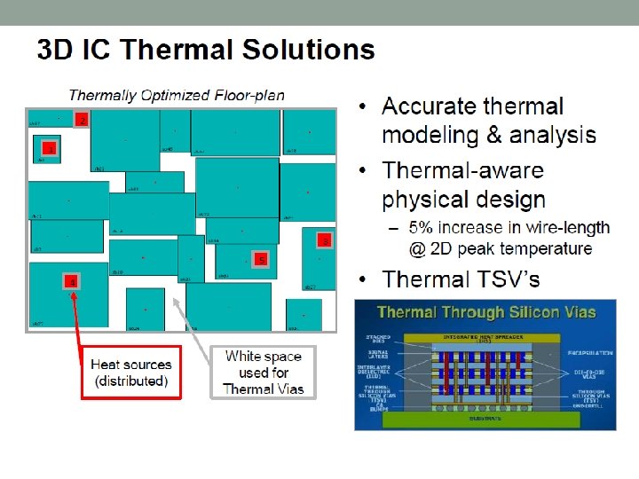
In summary • 3 D IC Yield • TSV fabrication causes thermal stress • Specified keep-away-zone needed for stress sensitive devices • Crack driving force induced (serious problem) • 3 D IC reliability (self-heating) • Thermomigration • Electromigration • TSV chips warpage • Self-heating simulations developed • Heat dissipation discussed
- Slides: 32