3 CMOS Transistor Theory Outline Introduction MOS Capacitor
- Slides: 19

3: CMOS Transistor Theory

Outline • Introduction • MOS Capacitor • n. MOS I-V Characteristics • p. MOS I-V Characteristics • Gate and Diffusion Capacitance Diseño de Circuitos Digitales para Comunicaciones 3: CMOS Transistor Theory 2

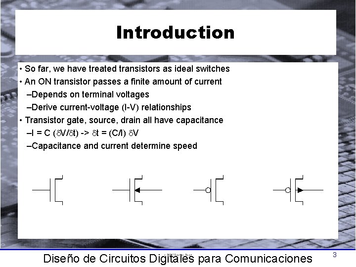
Introduction • So far, we have treated transistors as ideal switches • An ON transistor passes a finite amount of current –Depends on terminal voltages –Derive current-voltage (I-V) relationships • Transistor gate, source, drain all have capacitance –I = C (d. V/dt) -> dt = (C/I) d. V –Capacitance and current determine speed Diseño de Circuitos Digitales para Comunicaciones 3: CMOS Transistor Theory 3

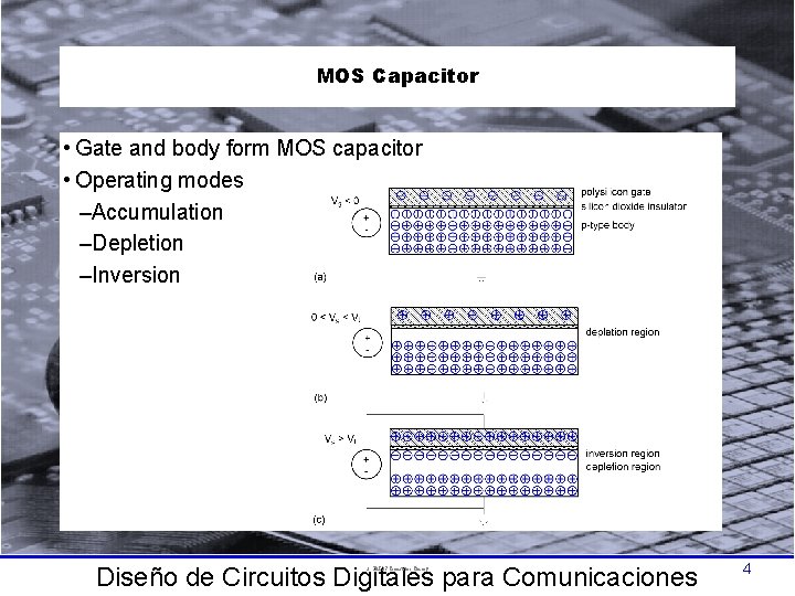
MOS Capacitor • Gate and body form MOS capacitor • Operating modes –Accumulation –Depletion –Inversion Diseño de Circuitos Digitales para Comunicaciones 3: CMOS Transistor Theory 4

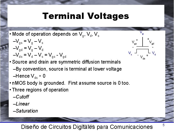
Terminal Voltages • Mode of operation depends on Vg, Vd, Vs –Vgs = Vg – Vs –Vgd = Vg – Vd –Vds = Vd – Vs = Vgs - Vgd • Source and drain are symmetric diffusion terminals –By convention, source is terminal at lower voltage –Hence Vds ≈ 0 • n. MOS body is grounded. First assume source is 0 too. • Three regions of operation –Cutoff –Linear –Saturation Diseño de Circuitos Digitales para Comunicaciones 3: CMOS Transistor Theory 5

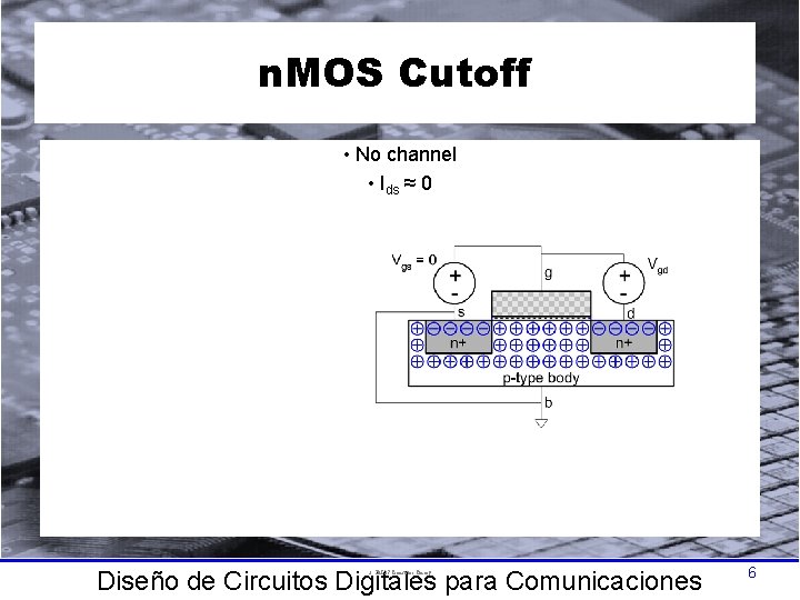
n. MOS Cutoff • No channel • Ids ≈ 0 Diseño de Circuitos Digitales para Comunicaciones 3: CMOS Transistor Theory 6

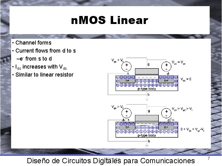
n. MOS Linear • Channel forms • Current flows from d to s –e- from s to d • Ids increases with Vds • Similar to linear resistor Diseño de Circuitos Digitales para Comunicaciones 3: CMOS Transistor Theory 7

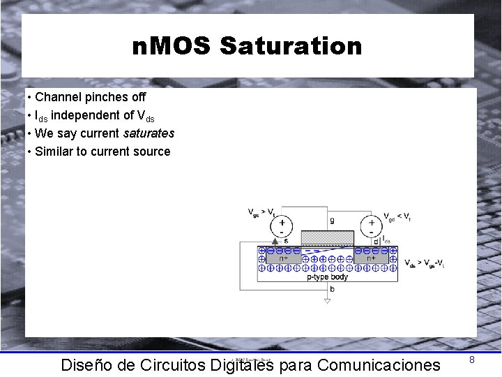
n. MOS Saturation • Channel pinches off • Ids independent of Vds • We say current saturates • Similar to current source Diseño de Circuitos Digitales para Comunicaciones 3: CMOS Transistor Theory 8

I-V Characteristics • In Linear region, Ids depends on –How much charge is in the channel? –How fast is the charge moving? Diseño de Circuitos Digitales para Comunicaciones 3: CMOS Transistor Theory 9

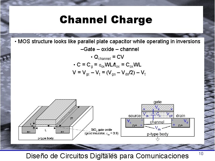
Channel Charge • MOS structure looks like parallel plate capacitor while operating in inversions –Gate – oxide – channel • Qchannel = CV • C = Cg = eox. WL/tox = Cox. WL • V = Vgc – Vt = (Vgs – Vds/2) – Vt Cox = eox / tox Diseño de Circuitos Digitales para Comunicaciones 3: CMOS Transistor Theory 10

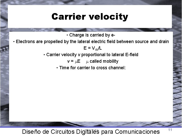
Carrier velocity • Charge is carried by e • Electrons are propelled by the lateral electric field between source and drain E = Vds/L • Carrier velocity v proportional to lateral E-field v = E called mobility • Time for carrier to cross channel: –t = L / v Diseño de Circuitos Digitales para Comunicaciones 3: CMOS Transistor Theory 11

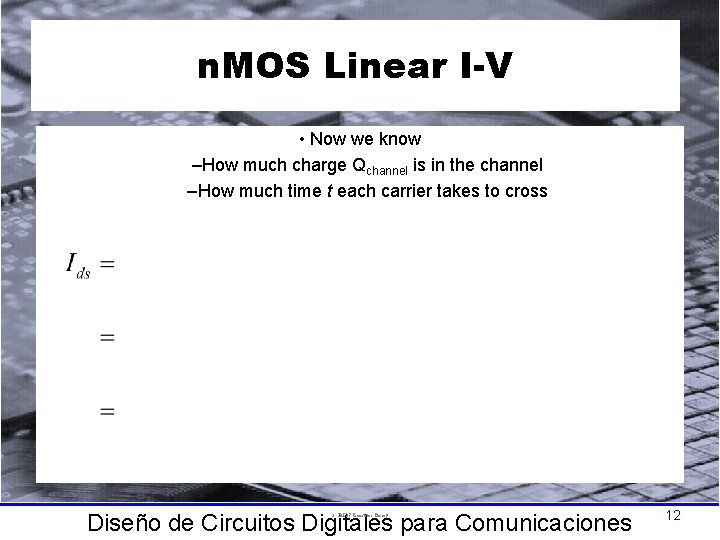
n. MOS Linear I-V • Now we know –How much charge Qchannel is in the channel –How much time t each carrier takes to cross Diseño de Circuitos Digitales para Comunicaciones 3: CMOS Transistor Theory 12

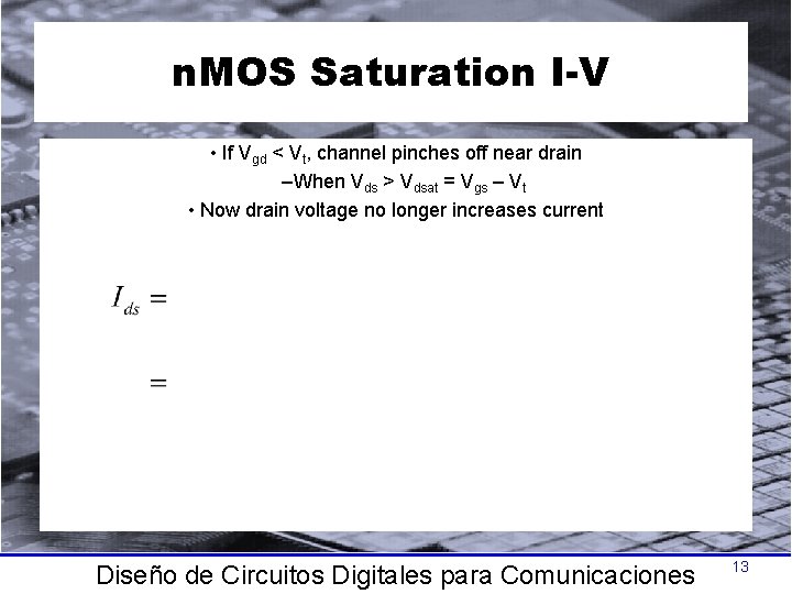
n. MOS Saturation I-V • If Vgd < Vt, channel pinches off near drain –When Vds > Vdsat = Vgs – Vt • Now drain voltage no longer increases current Diseño de Circuitos Digitales para Comunicaciones 13

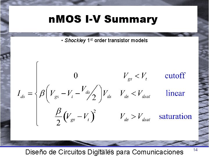
n. MOS I-V Summary • Shockley 1 st order transistor models Diseño de Circuitos Digitales para Comunicaciones 3: CMOS Transistor Theory 14

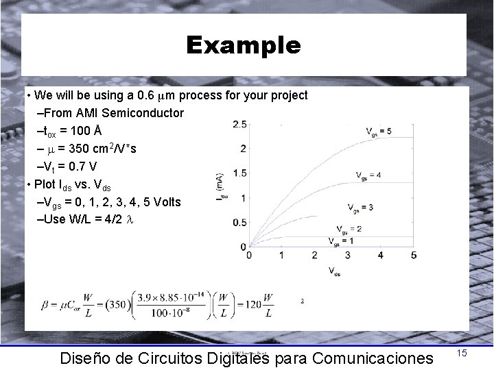
Example • We will be using a 0. 6 μm process for your project –From AMI Semiconductor –tox = 100 Å – = 350 cm 2/V*s –Vt = 0. 7 V • Plot Ids vs. Vds –Vgs = 0, 1, 2, 3, 4, 5 Volts –Use W/L = 4/2 Diseño de Circuitos Digitales para Comunicaciones 3: CMOS Transistor Theory 15

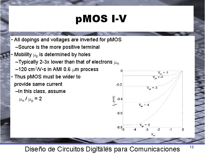
p. MOS I-V • All dopings and voltages are inverted for p. MOS –Source is the more positive terminal • Mobility p is determined by holes –Typically 2 -3 x lower than that of electrons n – 120 cm 2/V • s in AMI 0. 6 m process • Thus p. MOS must be wider to provide same current –In this class, assume n / p = 2 Diseño de Circuitos Digitales para Comunicaciones 3: CMOS Transistor Theory 16

Capacitance • Any two conductors separated by an insulator have capacitance • Gate to channel capacitor is very important –Creates channel charge necessary for operation • Source and drain have capacitance to body –Across reverse-biased diodes –Called diffusion capacitance because it is associated with source/drain diffusion Diseño de Circuitos Digitales para Comunicaciones 3: CMOS Transistor Theory 17

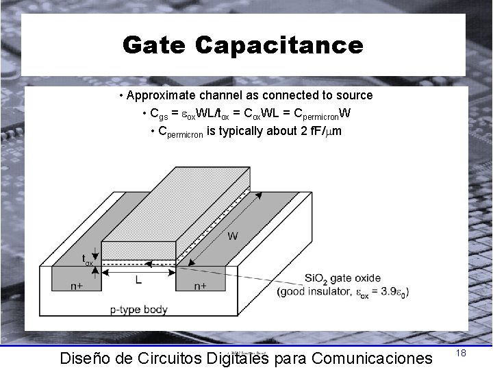
Gate Capacitance • Approximate channel as connected to source • Cgs = eox. WL/tox = Cox. WL = Cpermicron. W • Cpermicron is typically about 2 f. F/ m Diseño de Circuitos Digitales para Comunicaciones 3: CMOS Transistor Theory 18

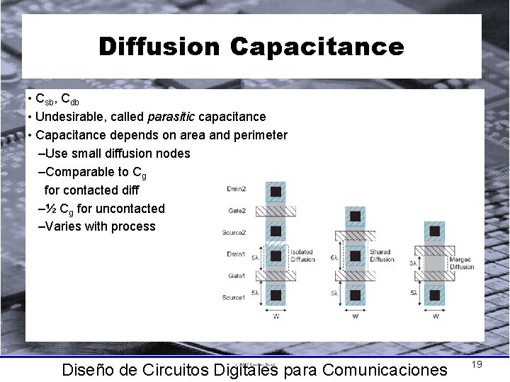
Diffusion Capacitance • Csb, Cdb • Undesirable, called parasitic capacitance • Capacitance depends on area and perimeter –Use small diffusion nodes –Comparable to Cg for contacted diff –½ Cg for uncontacted –Varies with process Diseño de Circuitos Digitales para Comunicaciones 3: CMOS Transistor Theory 19