24 bit Audio CODEC Digital Circuit Lab TA
24 -bit Audio CODEC Digital Circuit Lab TA: Po-Chen Wu
Outline • • Introduction to Audio Signal Architecture Overview Device Initialization Device Operation 2
Introduction to Audio Signal 3
Introduction • An audio signal is a representation of sound, typically as an electrical voltage. • Audio signals have frequencies in the audio frequency range of roughly 20 to 20, 000 Hz. • Audio signals may be synthesized directly, or may originate at a transducer such as a microphone. • Loudspeakers or headphones convert an electrical audio signal into sound. 4
Line Level (1/2) • Line level is the specified strength of an audio signal used to transmit analog sound between audio components. • As opposed to line level, there are weaker audio signals, such as those from microphones, and stronger signals, such as those used to drive headphones and loudspeakers. 5
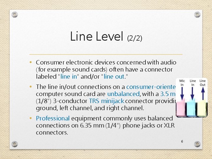
Line Level (2/2) • Consumer electronic devices concerned with audio (for example sound cards) often have a connector labeled "line in" and/or "line out. " • The line in/out connections on a consumer-oriented computer sound card are unbalanced, with a 3. 5 mm (1/8") 3 -conductor TRS minijack connector providing ground, left channel, and right channel. • Professional equipment commonly uses balanced connections on 6. 35 mm (1/4") phone jacks or XLR connectors. 6
Line In V. S. Mic In • A line input level signal typically has a voltage ranging from 0. 3 to 2 Volts. • A microphone input level signal is more often in the range from 5 to 50 m. V (millivolts). • Need microphone input level boost. 7
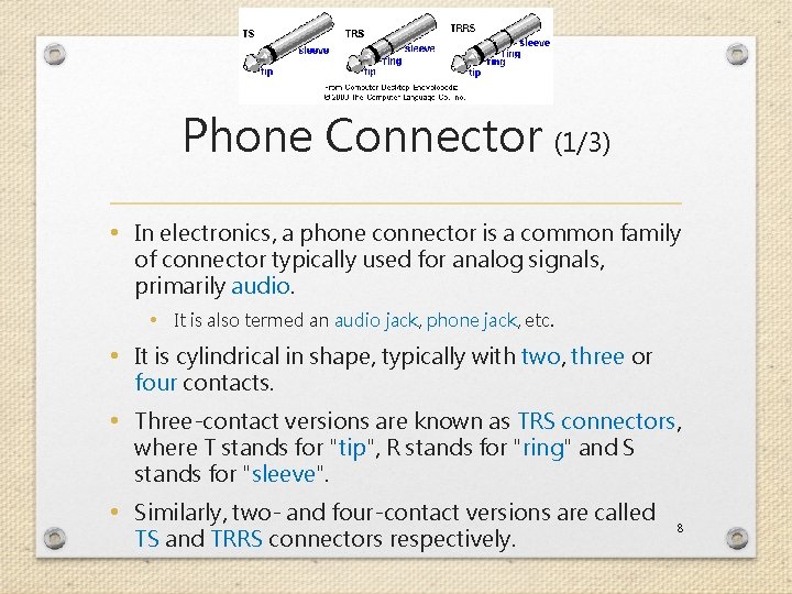
Phone Connector (1/3) • In electronics, a phone connector is a common family of connector typically used for analog signals, primarily audio. • It is also termed an audio jack, phone jack, etc. • It is cylindrical in shape, typically with two, three or four contacts. • Three-contact versions are known as TRS connectors, where T stands for "tip", R stands for "ring" and S stands for "sleeve". • Similarly, two- and four-contact versions are called TS and TRRS connectors respectively. 8
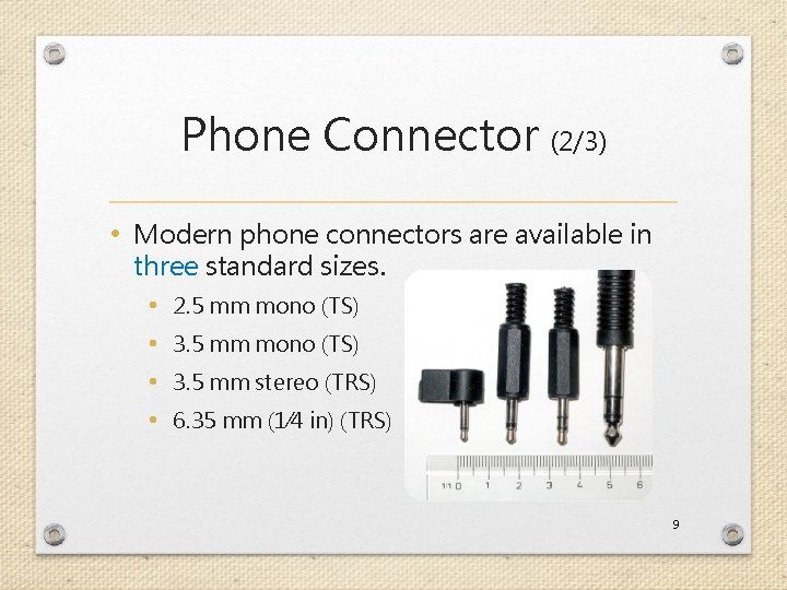
Phone Connector (2/3) • Modern phone connectors are available in three standard sizes. • 2. 5 mm mono (TS) • 3. 5 mm stereo (TRS) • 6. 35 mm (1⁄4 in) (TRS) 9
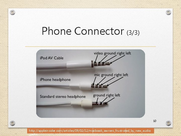
Phone Connector (3/3) 10 http: //appleinsider. com/articles/09/02/12/macbook_owners_frustrated_by_new_audio _jacks
Architecture Overview 11
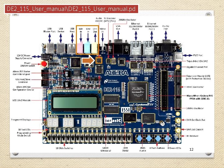
DE 2_115_User_manualDE 2_115_User_manual. pd f 12
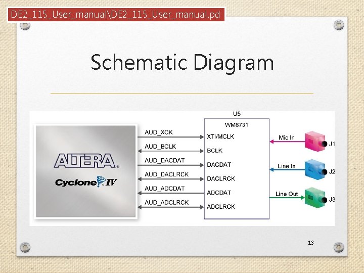
DE 2_115_User_manualDE 2_115_User_manual. pd f Schematic Diagram 13
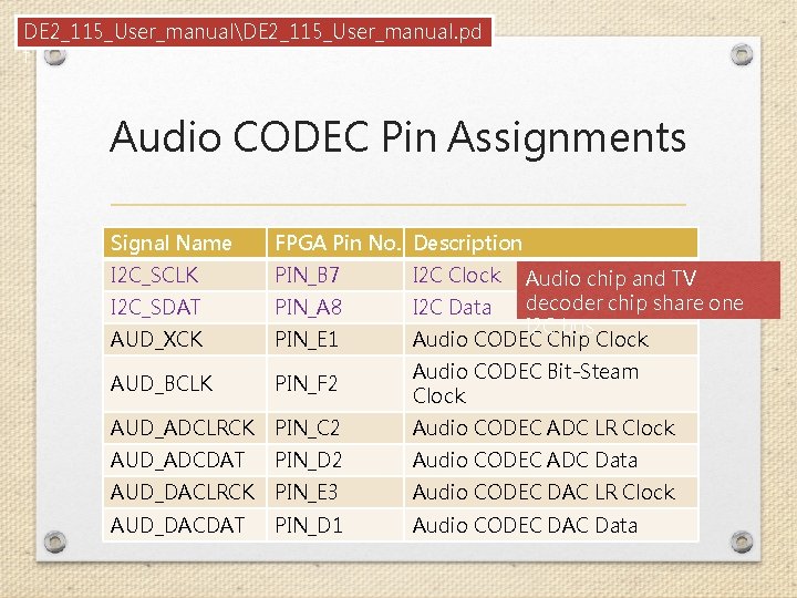
DE 2_115_User_manualDE 2_115_User_manual. pd f Audio CODEC Pin Assignments Signal Name FPGA Pin No. Description I 2 C_SCLK PIN_B 7 I 2 C_SDAT PIN_A 8 AUD_XCK PIN_E 1 AUD_BCLK PIN_F 2 Audio CODEC Bit-Steam Clock AUD_ADCLRCK PIN_C 2 Audio CODEC ADC LR Clock AUD_ADCDAT PIN_D 2 Audio CODEC ADC Data AUD_DACLRCK PIN_E 3 Audio CODEC DAC LR Clock AUD_DACDAT PIN_D 1 Audio CODEC DAC Data I 2 C Clock Audio chip and TV decoder chip share one I 2 C Data I 2 C bus Audio CODEC Chip Clock 14
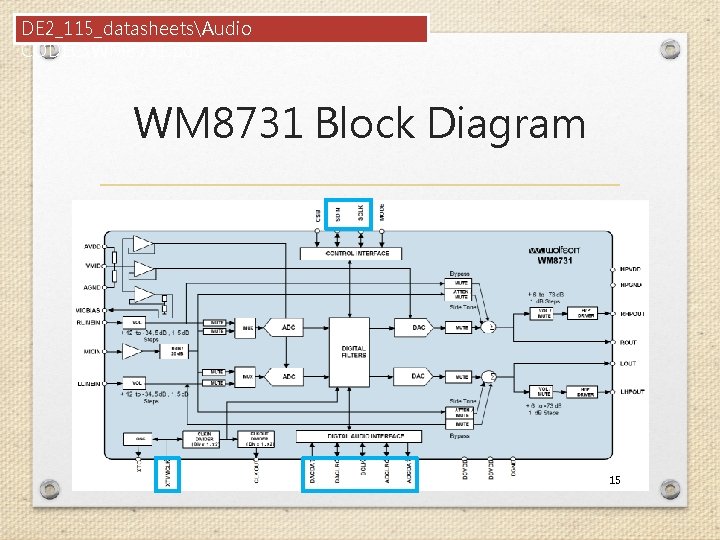
DE 2_115_datasheetsAudio CODECWM 8731. pdf WM 8731 Block Diagram 15
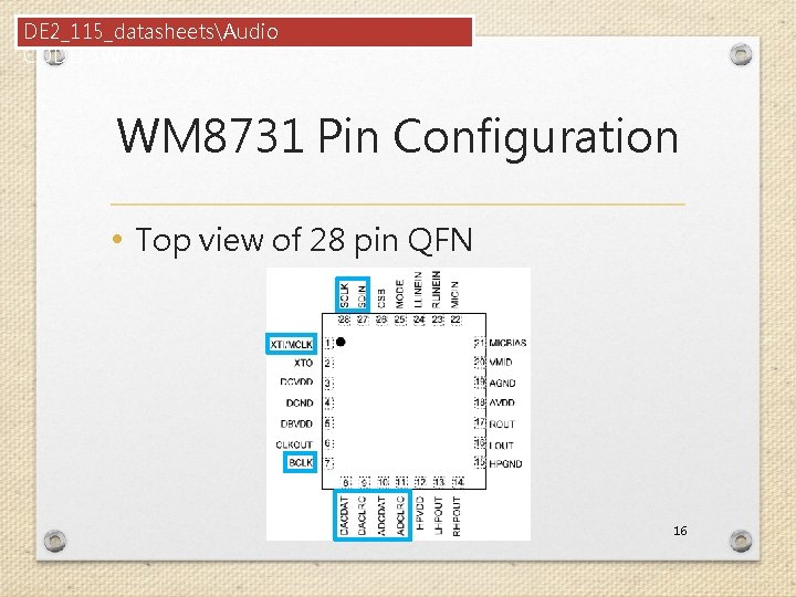
DE 2_115_datasheetsAudio CODECWM 8731. pdf WM 8731 Pin Configuration • Top view of 28 pin QFN 16
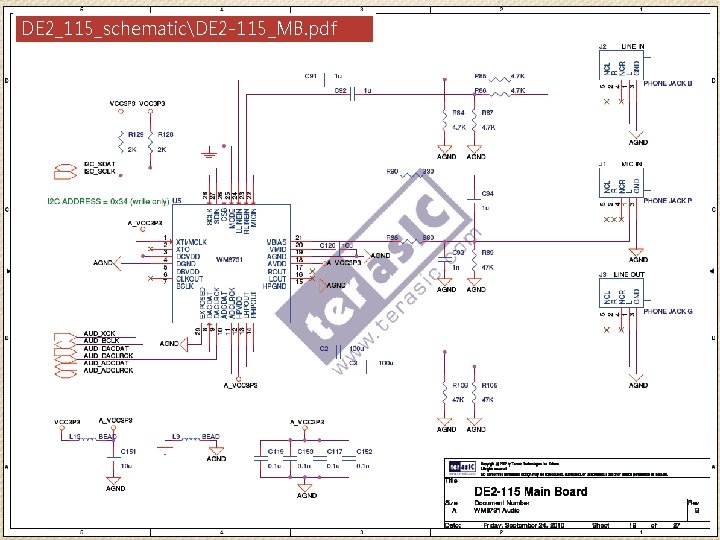
DE 2_115_schematicDE 2 -115_MB. pdf 17
How to Use WM 8731? 1. Initialize the device by setting the registers via I 2 C bus interface. 2. After correct initialization, we can receive or transmit audio data via digital audio interface. 18
Device Initialization 19
Software Control Interface (1/2) • Different modes can be configured under software control. • Input to ADC: Microphone • Sampling rate: 32 k. Hz • Input audio data bit length: 16 bits • etc. 20
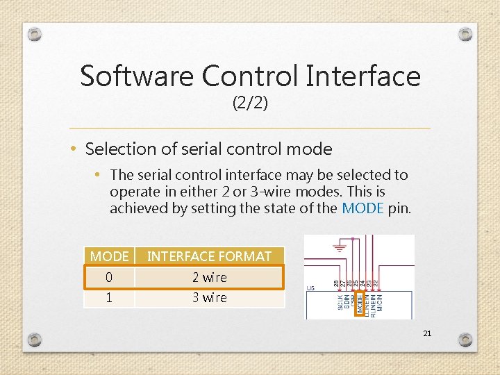
Software Control Interface (2/2) • Selection of serial control mode • The serial control interface may be selected to operate in either 2 or 3 -wire modes. This is achieved by setting the state of the MODE pin. MODE INTERFACE FORMAT 0 2 wire 1 3 wire 21
2 -Wire Serial Control Mode • The WM 8731/L supports a 2 -wire MPU (Microprocessor unit) interface, which is compatible with I²C protocol. • I²C (Inter-Integrated Circuit, referred to as I- squared-C) uses only two bidirectional opendrain lines, Serial Data Line (SDA) and Serial Clock (SCL). 22
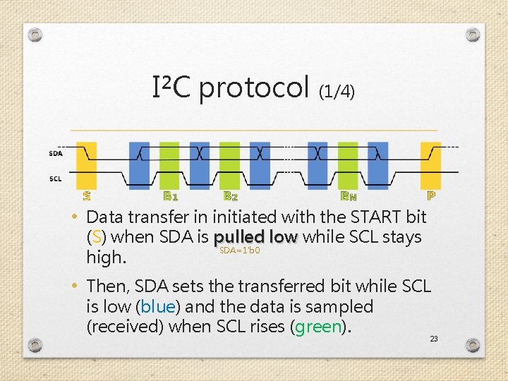
I²C protocol (1/4) • Data transfer in initiated with the START bit (S) when SDA is pulled low while SCL stays SDA=1'b 0 high. • Then, SDA sets the transferred bit while SCL is low (blue) and the data is sampled (received) when SCL rises (green). 23
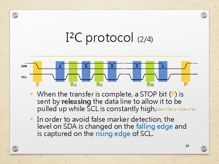
I²C protocol (2/4) • When the transfer is complete, a STOP bit (P) is sent by releasing the data line to allow it to be pulled up while SCL is constantly high. SDA=1'b 1 or SDA=1'bz • In order to avoid false marker detection, the level on SDA is changed on the falling edge and is captured on the rising edge of SCL. 24
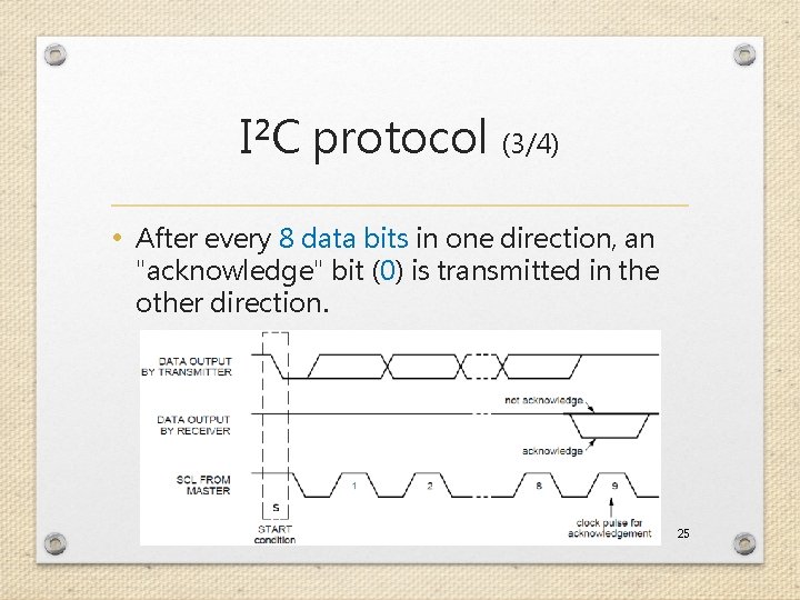
I²C protocol (3/4) • After every 8 data bits in one direction, an "acknowledge" bit (0) is transmitted in the other direction. 25
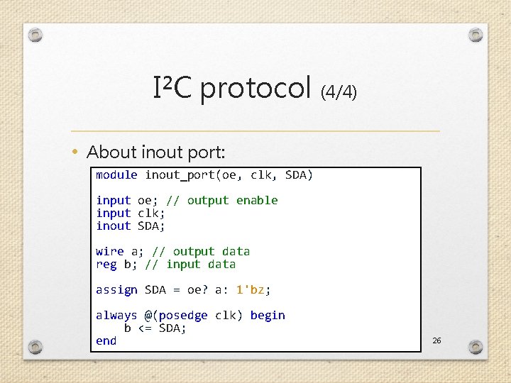
I²C protocol (4/4) • About inout port: module inout_port(oe, clk, SDA) input oe; // output enable input clk; inout SDA; wire a; // output data reg b; // input data assign SDA = oe? a: 1'bz; always @(posedge clk) begin b <= SDA; end 26
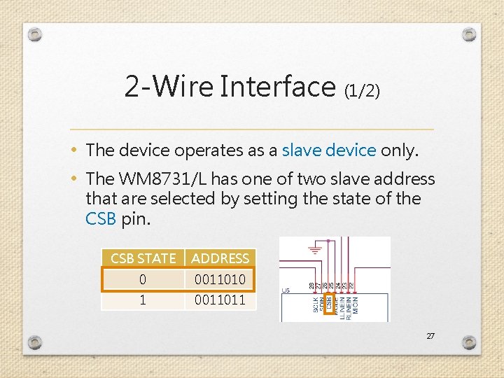
2 -Wire Interface (1/2) • The device operates as a slave device only. • The WM 8731/L has one of two slave address that are selected by setting the state of the CSB pin. CSB STATE ADDRESS 0 0011010 1 0011011 27
![2 -Wire Interface (2/2) • 2 -wire serial interface • • ADDR[6: 0] (7 2 -Wire Interface (2/2) • 2 -wire serial interface • • ADDR[6: 0] (7](http://slidetodoc.com/presentation_image_h/da89913d8bc0ae4c518eb7cd633330cd/image-28.jpg)
2 -Wire Interface (2/2) • 2 -wire serial interface • • ADDR[6: 0] (7 bits) are Slave Address Bits R/W is '0', indicating a write B[15: 9] (7 bits) are Register Address Bits B[8: 0] (9 bits) are Register Data Bits 0011010 0 Max freq. = 526 k. Hz 28
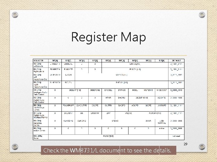
Register Map 29 Check the WM 8731/L document to see the details.
![Left Line In REGISTER BIT[8] BIT[7] BIT[6] BIT[5] R 0 (00 h) Left Line Left Line In REGISTER BIT[8] BIT[7] BIT[6] BIT[5] R 0 (00 h) Left Line](http://slidetodoc.com/presentation_image_h/da89913d8bc0ae4c518eb7cd633330cd/image-30.jpg)
Left Line In REGISTER BIT[8] BIT[7] BIT[6] BIT[5] R 0 (00 h) Left Line In LRINBOTH LINMUTE 0 0 BIT[4] BIT[3] BIT[2] BIT[1] BIT[0] LINVOL[4: 0] DEFAULT 0_1001_0111 • Just use the default setting if we do not use the line input. • 000_0_1001_0111 30
![Right Line In REGISTER BIT[8] BIT[7] BIT[6] BIT[5] R 1 (01 h) Right Line Right Line In REGISTER BIT[8] BIT[7] BIT[6] BIT[5] R 1 (01 h) Right Line](http://slidetodoc.com/presentation_image_h/da89913d8bc0ae4c518eb7cd633330cd/image-31.jpg)
Right Line In REGISTER BIT[8] BIT[7] BIT[6] BIT[5] R 1 (01 h) Right Line In RLINBOTH RINMUTE 0 0 BIT[4] BIT[3] BIT[2] BIT[1] BIT[0] RINVOL[4: 0] DEFAULT 0_1001_0111 • Just use the default setting if we do not use the line input. • 000_0001_0_1001_0111 31
![Left Headphone Out REGISTER BIT[8] BIT[7] R 2 (02 h) Left Headphone Out LRHPBOTH Left Headphone Out REGISTER BIT[8] BIT[7] R 2 (02 h) Left Headphone Out LRHPBOTH](http://slidetodoc.com/presentation_image_h/da89913d8bc0ae4c518eb7cd633330cd/image-32.jpg)
Left Headphone Out REGISTER BIT[8] BIT[7] R 2 (02 h) Left Headphone Out LRHPBOTH LZCEN BIT[6] BIT[5] BIT[4] BIT[3] BIT[2] BIT[1] BIT[0] LHPVOL[6: 0] DEFAULT 0_0111_1001 • Here we can just use the default setting. • 000_0010_0_0111_1001 32
![Right Headphone Out REGISTER BIT[8] BIT[7] R 3 (03 h) Right Headphone Out RLHPBOTH Right Headphone Out REGISTER BIT[8] BIT[7] R 3 (03 h) Right Headphone Out RLHPBOTH](http://slidetodoc.com/presentation_image_h/da89913d8bc0ae4c518eb7cd633330cd/image-33.jpg)
Right Headphone Out REGISTER BIT[8] BIT[7] R 3 (03 h) Right Headphone Out RLHPBOTH RZCEN BIT[6] BIT[5] BIT[4] BIT[3] BIT[2] BIT[1] BIT[0] RHPVOL[6: 0] DEFAULT 0_0111_1001 • Here we can just use the default setting. • 000_0011_0_0111_1001 33
![Analogue Audio Path Control REGISTER BIT[8] R 4 (04 h) Analogue Audio Path Control Analogue Audio Path Control REGISTER BIT[8] R 4 (04 h) Analogue Audio Path Control](http://slidetodoc.com/presentation_image_h/da89913d8bc0ae4c518eb7cd633330cd/image-34.jpg)
Analogue Audio Path Control REGISTER BIT[8] R 4 (04 h) Analogue Audio Path Control 0 BIT[7] BIT[6] SIDEATT[1: 0] BIT[5] BIT[4] BIT[3] BIT[2] BIT[1] BIT[0] DEFAULT SIDETONE DACSEL BYPASS INSEL MUTEMIC MICBOOST 0_0000_1010 • Enable boost, disable mute, choose microphone input, disable bypass, and select DAC. • 000_0100_0_0001_0101 34
![Digital Audio Path Control REGISTER BIT[8] BIT[7] BIT[6] BIT[5] BIT[4] BIT[3] R 5 (05 Digital Audio Path Control REGISTER BIT[8] BIT[7] BIT[6] BIT[5] BIT[4] BIT[3] R 5 (05](http://slidetodoc.com/presentation_image_h/da89913d8bc0ae4c518eb7cd633330cd/image-35.jpg)
Digital Audio Path Control REGISTER BIT[8] BIT[7] BIT[6] BIT[5] BIT[4] BIT[3] R 5 (05 h) Digital Audio Path Control 0 0 HPOR DACMU BIT[2] BIT[1] DEEMPH[1: 0] BIT[0] DEFAULT ADCHPD 0_0000_1000 • Disable soft mute • 000_0101_0_0000 35
![Power Down Control REGISTER BIT[8] BIT[7] BIT[6] BIT[5] BIT[4] BIT[3] BIT[2] BIT[1] BIT[0] DEFAULT Power Down Control REGISTER BIT[8] BIT[7] BIT[6] BIT[5] BIT[4] BIT[3] BIT[2] BIT[1] BIT[0] DEFAULT](http://slidetodoc.com/presentation_image_h/da89913d8bc0ae4c518eb7cd633330cd/image-36.jpg)
Power Down Control REGISTER BIT[8] BIT[7] BIT[6] BIT[5] BIT[4] BIT[3] BIT[2] BIT[1] BIT[0] DEFAULT R 6 (06 h) Power Down Control 0 POWER OFF CLKOUTPD OSCPD OUTPD DACPD ADCPD MICPD LINEINPD 0_1001_1111 • Choose power on and disable all the power down options. • 000_0110_0_0000 36
![Digital Audio Interface Format (1/2) REGISTER BIT[8] BIT[7] BIT[6] BIT[5] BIT[4] R 7 (07 Digital Audio Interface Format (1/2) REGISTER BIT[8] BIT[7] BIT[6] BIT[5] BIT[4] R 7 (07](http://slidetodoc.com/presentation_image_h/da89913d8bc0ae4c518eb7cd633330cd/image-37.jpg)
Digital Audio Interface Format (1/2) REGISTER BIT[8] BIT[7] BIT[6] BIT[5] BIT[4] R 7 (07 h) Digital Audio Interface Format 0 BCLKIVE MS LRSWAP LRP BIT[3] BIT[2] IWL[[1: 0] BIT[1] BIT[0] FORMAT[1: 0] DEFAULT 0_0000_1010 • Choose I 2 S format, 16 -bit length, and master mode. • 000_0111_0_0100_0010 37
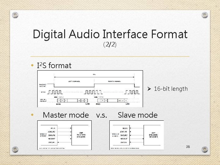
Digital Audio Interface Format (2/2) • I 2 S format Ø 16 -bit length • Master mode v. s. Slave mode 38
![Sampling Control (1/2) REGISTER BIT[8] BIT[7] BIT[6] R 8 (08 h) Sampling Control 0 Sampling Control (1/2) REGISTER BIT[8] BIT[7] BIT[6] R 8 (08 h) Sampling Control 0](http://slidetodoc.com/presentation_image_h/da89913d8bc0ae4c518eb7cd633330cd/image-39.jpg)
Sampling Control (1/2) REGISTER BIT[8] BIT[7] BIT[6] R 8 (08 h) Sampling Control 0 CLKODIV 2 CLKIDIV 2 BIT[5] BIT[4] BIT[3] SR[3: 0] BIT[2] BIT[1] BIT[0] DEFAULT BOSR USB/ Normal 0_0000 • Choose USB mode (fixed MCLK 12 MHz) and sampling rate = 32 k. Hz. • 000_1000_0_0001_ 01 100 10 1 39
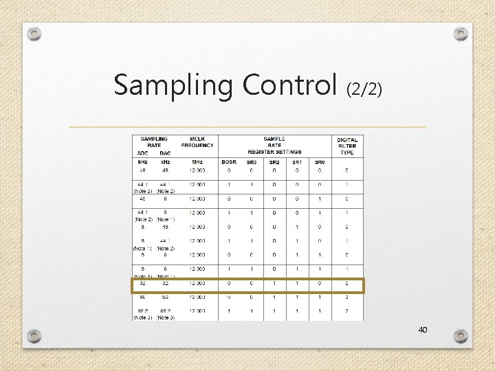
Sampling Control (2/2) 40
![Active Control REGISTER BIT[8] BIT[7] BIT[6] BIT[5] BIT[4] BIT[3] BIT[2] BIT[1] BIT[0] DEFAULT R Active Control REGISTER BIT[8] BIT[7] BIT[6] BIT[5] BIT[4] BIT[3] BIT[2] BIT[1] BIT[0] DEFAULT R](http://slidetodoc.com/presentation_image_h/da89913d8bc0ae4c518eb7cd633330cd/image-41.jpg)
Active Control REGISTER BIT[8] BIT[7] BIT[6] BIT[5] BIT[4] BIT[3] BIT[2] BIT[1] BIT[0] DEFAULT R 9 (09 h) Active Control 0 0 0 0 Active 0_0000 • Activate interface • 000_1001_0_0001 41
![Reset Register REGISTER R 15 (15 h) Active Control BIT[8] BIT[7] BIT[6] BIT[5] BIT[4] Reset Register REGISTER R 15 (15 h) Active Control BIT[8] BIT[7] BIT[6] BIT[5] BIT[4]](http://slidetodoc.com/presentation_image_h/da89913d8bc0ae4c518eb7cd633330cd/image-42.jpg)
Reset Register REGISTER R 15 (15 h) Active Control BIT[8] BIT[7] BIT[6] BIT[5] BIT[4] BIT[3] BIT[2] BIT[1] BIT[0] RESET[8: 0] DEFAULT not reset • You can try to reset the device to a known (? ) state. • 000_1111_0_0000 (? ) 42
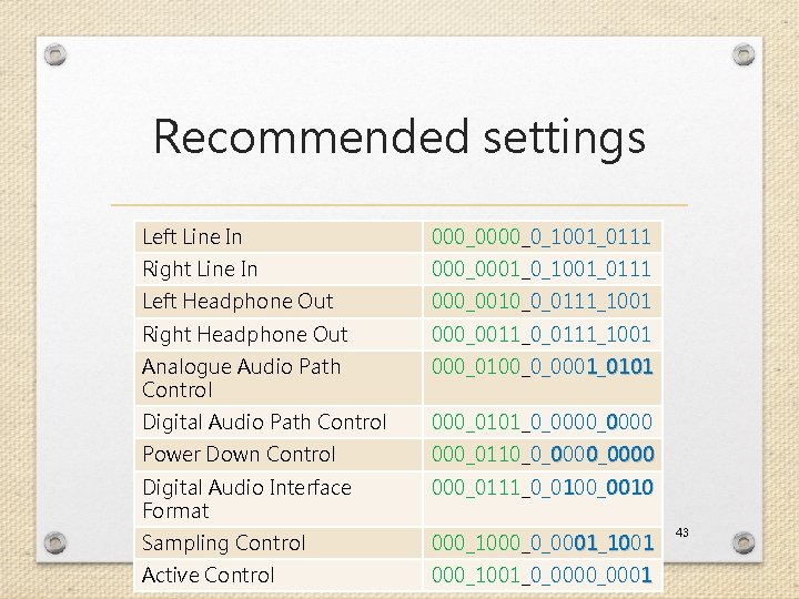
Recommended settings Left Line In 000_0_1001_0111 Right Line In 000_0001_0_1001_0111 Left Headphone Out 000_0010_0_0111_1001 Right Headphone Out 000_0011_0_0111_1001 Analogue Audio Path Control 000_0100_0_0001_0101 Digital Audio Path Control 000_0101_0_0000 Power Down Control 000_0110_0_0000 Digital Audio Interface Format 000_0111_0_0100_0010 Sampling Control 000_1000_0_0001_ 01 100 10 1 Active Control 000_1001_0_0001 43
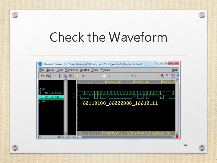
Check the Waveform 00110100_0000_10010111 44
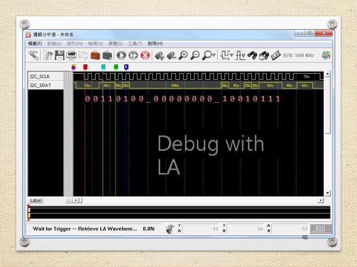
00110100_0000_10010111 Debug with LA 45
Device Operation 46
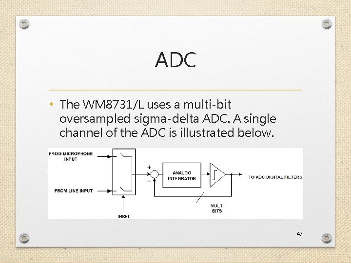
ADC • The WM 8731/L uses a multi-bit oversampled sigma-delta ADC. A single channel of the ADC is illustrated below. 47
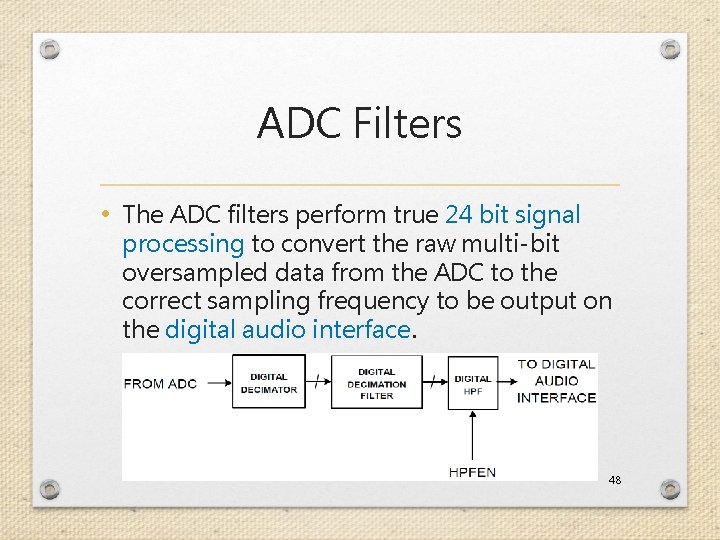
ADC Filters • The ADC filters perform true 24 bit signal processing to convert the raw multi-bit oversampled data from the ADC to the correct sampling frequency to be output on the digital audio interface. 48
Digital Audio Interfaces (1/5) • WM 8731/L may be operated in either one of the 4 offered audio interface modes. These are: • Right justified • Left justified • I 2 S • DSP mode • All four of these modes are MSB first and operate with data 16 to 32 bits. 49
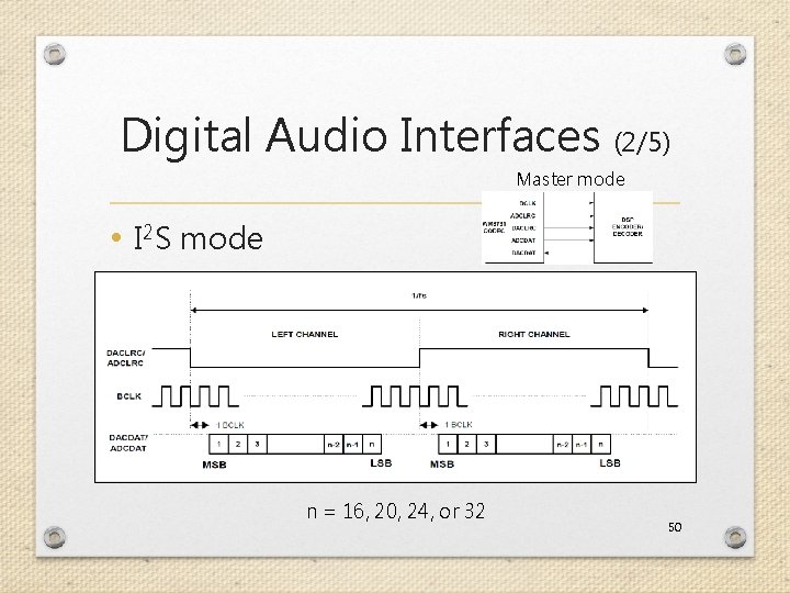
Digital Audio Interfaces (2/5) Master mode • I 2 S mode n = 16, 20, 24, or 32 50
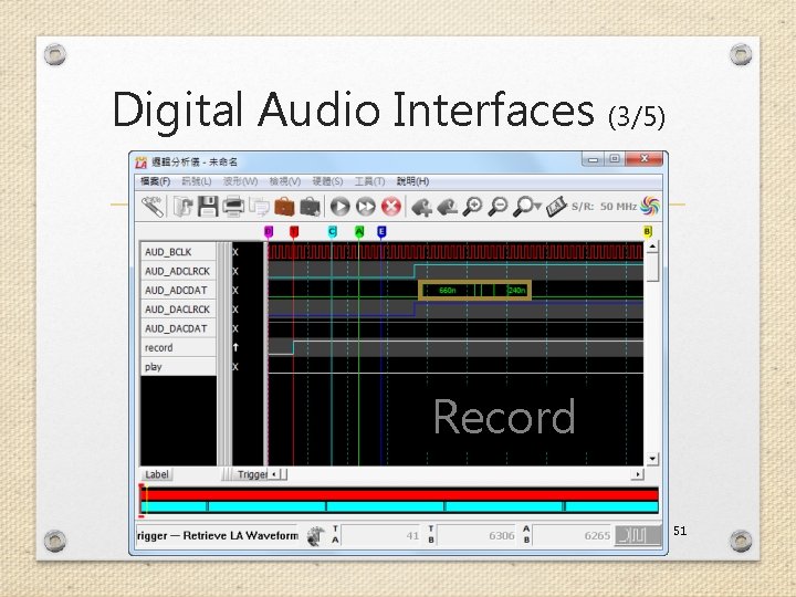
Digital Audio Interfaces (3/5) Record 51
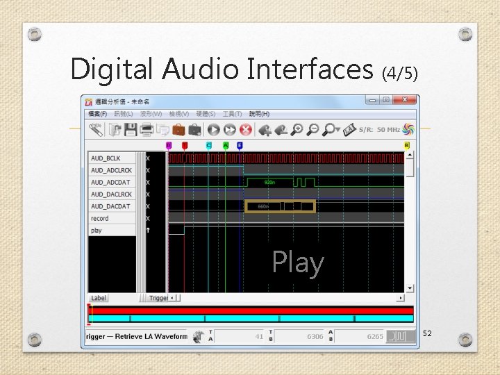
Digital Audio Interfaces (4/5) Play 52
Digital Audio Interfaces (5/5) • The length of the digital audio data is programmable at 16/20/24 or 32 bits. • The data is signed 2's complement. • If the ADC is programmed to output 16 or 20 bit data then it strips the LSBs from the 24 bit data. • If the ADC is programmed to output 32 bits then it packs the LSBs with zeros. • Similar adjustments in DAC. 53
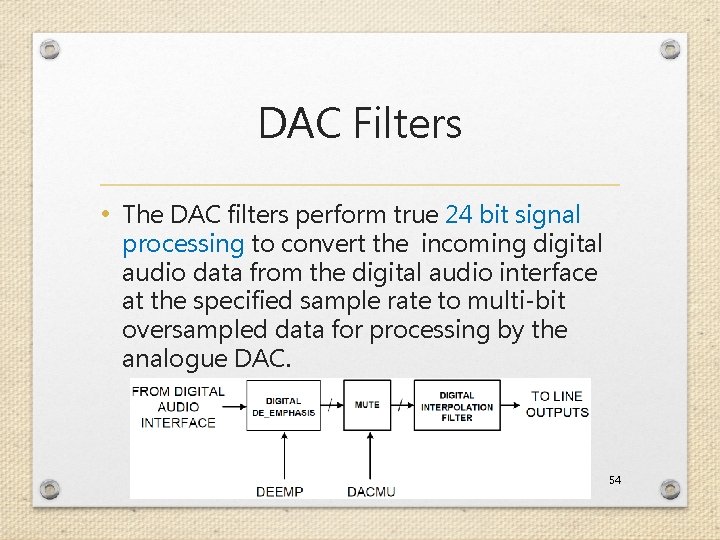
DAC Filters • The DAC filters perform true 24 bit signal processing to convert the incoming digital audio data from the digital audio interface at the specified sample rate to multi-bit oversampled data for processing by the analogue DAC. 54
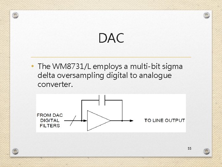
DAC • The WM 8731/L employs a multi-bit sigma delta oversampling digital to analogue converter. 55
The End. Any question?
Reference 1. http: //en. wikipedia. org/wiki/Audio_sign 2. 3. 4. 5. 6. al http: //en. wikipedia. org/wiki/I%C 2%B 2 C "THE I 2 C-BUS SPECIFICATION VERSION 2. 1" by Philips. "DE 2 -115 User Manual" by Terasic. "DE 2 -115_MB. pdf" by Terasic. "WM 8731. pdf" by Wolfson Microelectronics. 57
- Slides: 57