2140707 Computer Organization Unit2 Basic Computer Organization and
2140707 Computer Organization Unit-2 Basic Computer Organization and Design Prof. Hardik A. Doshi 99789 11553 hardik. doshi@darshan. ac. in
Topics to be covered § Instruction codes § Computer registers § Computer instructions § Timing and Control § Instruction cycle § Memory‐Reference Instructions § Input‐output and interrupt § Complete computer description § Design of Basic computer § Design of Accumulator Unit – 2: Basic Computer Organization 2 Darshan Institute of Engineering & Technology
Instruction codes Unit – 2: Basic Computer Organization Darshan Institute of Engineering & Technology
Instruction Codes § Program • A program is a set of instructions that specify the operations, operands and the sequence by which processing has to occur. § Computer Instruction • A computer instruction is a binary code that specifies a sequence of microoperations for the computer. • The computer reads each instruction from memory and places it in a control register. • The control then interprets the binary code of the instruction and proceeds to execute it by issuing a sequence of microoperations. Unit – 2: Basic Computer Organization 4 Darshan Institute of Engineering & Technology
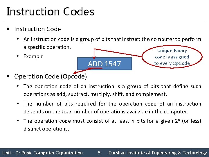
Instruction Codes § Instruction Code • An instruction code is a group of bits that instruct the computer to perform a specific operation. • Example ADD 1547 Unique Binary code is assigned to every Op. Code § Operation Code (Opcode) • The operation code of an instruction is a group of bits that define such operations as add, subtract, multiply, shift, and complement. • The number of bits required for the operation code of an instruction depends on the total number of operations available in the computer. • The operation code must consist of at least n bits for a given 2 n (or less) distinct operations. Unit – 2: Basic Computer Organization 5 Darshan Institute of Engineering & Technology
Stored Program Organization § The simplest way to organize a computer is to have one processor register(AC) and an instruction code format with two parts. § The first part specifies the operation (opcode) to be performed and the second specifies an address (operand). § The memory address tells the control where to find an operand in memory. § This operand is read from memory and used as the data to be operated on together with the data stored in the processor register. Unit – 2: Basic Computer Organization 6 Darshan Institute of Engineering & Technology
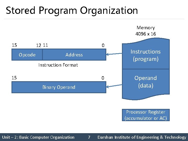
Stored Program Organization Memory 4096 x 16 15 12 11 Opcode 0 Address Instruction Format 15 0 Binary Operand Instructions (program) Operand (data) Processor Register (accumulator or AC) Unit – 2: Basic Computer Organization 7 Darshan Institute of Engineering & Technology
Stored Program Organization § Instructions are stored in one section of memory and data in another. § For a memory unit with 4096 words, we need 12 bits to specify an address since 212 = 4096. § If we store each instruction code in one 16‐bit memory word, we have available four bits for operation code (opcode) to specify one out of 16 possible operations, and 12 bits to specify the address of an operand. Unit – 2: Basic Computer Organization 8 Darshan Institute of Engineering & Technology
Stored Program Organization § The control reads a 16‐bit instruction from the program portion of memory. § It uses the 12‐bit address part of the instruction to read a 16‐bit operand from the data portion of memory. § It then executes the operation specified by the operation code. Unit – 2: Basic Computer Organization 9 Darshan Institute of Engineering & Technology
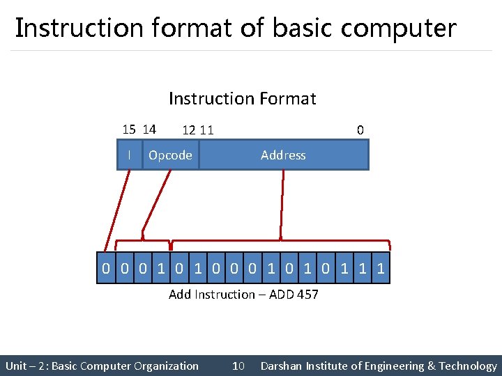
Instruction format of basic computer Instruction Format 15 14 I 12 11 0 Address Opcode 0 0 0 1 0 1 0 1 1 1 Add Instruction – ADD 457 Unit – 2: Basic Computer Organization 10 Darshan Institute of Engineering & Technology
Direct & Indirect Addressing of Memory § If the second part of an instruction format specifies the address of an operand, the instruction is said to have a direct address. § In Indirect address, the bits in the second part of the instruction designate an address of a memory word in which the address of the operand is found. Unit – 2: Basic Computer Organization 11 Darshan Institute of Engineering & Technology
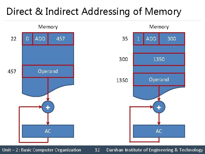
Direct & Indirect Addressing of Memory 22 457 0 ADD Memory 35 457 1 ADD 300 1350 Operand + + AC AC Unit – 2: Basic Computer Organization 12 Darshan Institute of Engineering & Technology
Direct & Indirect Addressing of Memory § One bit of the instruction code can be used to distinguish between a direct and an indirect address. § It consists of a 3‐bit operation code, a 12‐bit address, and an indirect address mode bit designated by I. § The mode bit is 0 for a direct address and 1 for an indirect address. Unit – 2: Basic Computer Organization 13 Darshan Institute of Engineering & Technology
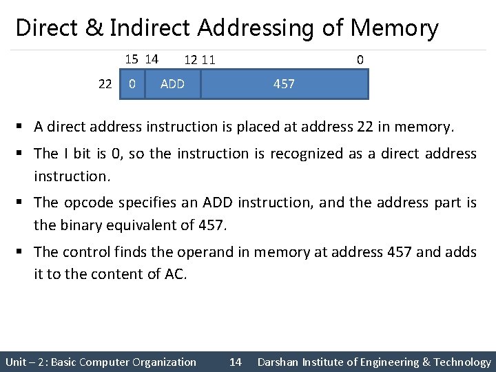
Direct & Indirect Addressing of Memory 15 14 22 0 12 11 0 457 ADD § A direct address instruction is placed at address 22 in memory. § The I bit is 0, so the instruction is recognized as a direct address instruction. § The opcode specifies an ADD instruction, and the address part is the binary equivalent of 457. § The control finds the operand in memory at address 457 and adds it to the content of AC. Unit – 2: Basic Computer Organization 14 Darshan Institute of Engineering & Technology
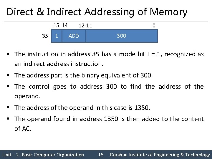
Direct & Indirect Addressing of Memory 15 14 35 1 12 11 0 300 ADD § The instruction in address 35 has a mode bit I = 1, recognized as an indirect address instruction. § The address part is the binary equivalent of 300. § The control goes to address 300 to find the address of the operand. § The address of the operand in this case is 1350. § The operand found in address 1350 is then added to the content of AC. Unit – 2: Basic Computer Organization 15 Darshan Institute of Engineering & Technology
Direct & Indirect Addressing of Memory § The indirect address instruction needs two references to memory to fetch an operand. § The first reference is needed to read the address of the operand. § Second reference is for the operand itself. § The memory word that holds the address of the operand in an indirect address instruction is used as a pointer to an array of data. Unit – 2: Basic Computer Organization 16 Darshan Institute of Engineering & Technology
Computer Registers Unit – 2: Basic Computer Organization Darshan Institute of Engineering & Technology
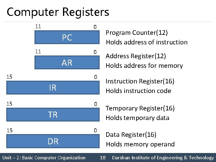
Computer Registers 11 0 Program Counter(12) Holds address of instruction PC 11 0 Address Register(12) Holds address for memory AR 15 0 Instruction Register(16) Holds instruction code IR 15 0 Temporary Register(16) Holds temporary data TR 15 0 Data Register(16) Holds memory operand DR Unit – 2: Basic Computer Organization 18 Darshan Institute of Engineering & Technology
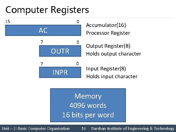
Computer Registers 15 0 Accumulator(16) Processor Register AC 7 0 Output Register(8) Holds output character OUTR 0 7 Input Register(8) Holds input character INPR Memory 4096 words 16 bits per word Unit – 2: Basic Computer Organization 19 Darshan Institute of Engineering & Technology
Common bus system of basic computer § Common bus Unit – 2: Basic Computer Organization 20 Darshan Institute of Engineering & Technology
Computer Instructions Unit – 2: Basic Computer Organization Darshan Institute of Engineering & Technology
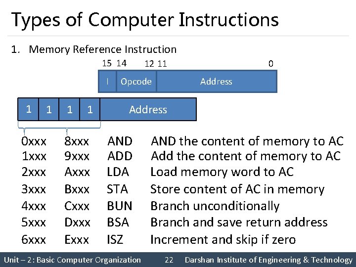
Types of Computer Instructions 1. Memory Reference Instruction 15 14 I 01 01 0 xxx 1 xxx 2 xxx 3 xxx 4 xxx 5 xxx 6 xxx 01 01 8 xxx 9 xxx Axxx Bxxx Cxxx Dxxx Exxx 12 11 0 Address Opcode Address AND ADD LDA STA BUN BSA ISZ Unit – 2: Basic Computer Organization AND the content of memory to AC Add the content of memory to AC Load memory word to AC Store content of AC in memory Branch unconditionally Branch and save return address Increment and skip if zero 22 Darshan Institute of Engineering & Technology
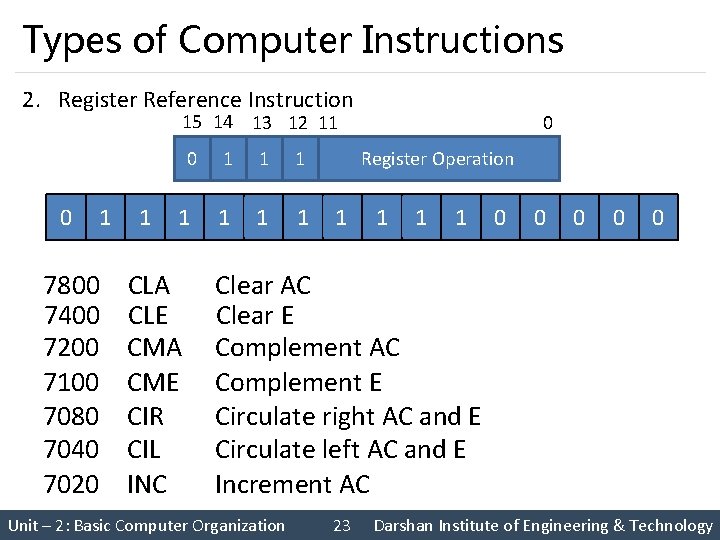
Types of Computer Instructions 2. Register Reference Instruction 15 14 13 12 11 0 0 1 7800 7400 7200 7100 7080 7040 7020 1 1 CLA CLE CMA CME CIR CIL INC 1 1 0 10 1 0 0 Register Operation 10 1 0 10 01 0 0 0 Clear AC Clear E Complement AC Complement E Circulate right AC and E Circulate left AC and E Increment AC Unit – 2: Basic Computer Organization 23 Darshan Institute of Engineering & Technology
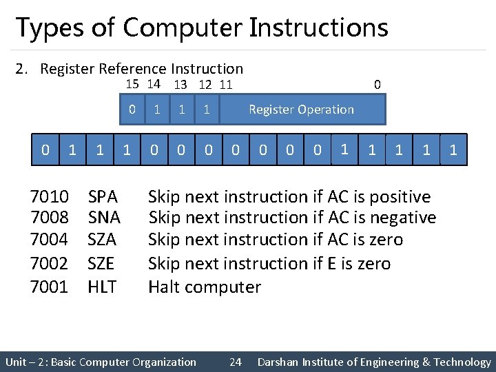
Types of Computer Instructions 2. Register Reference Instruction 15 14 13 12 11 0 0 1 7010 7008 7004 7002 7001 1 SPA SNA SZE HLT 1 1 0 0 Register Operation 0 0 10 01 10 Skip next instruction if AC is positive Skip next instruction if AC is negative Skip next instruction if AC is zero Skip next instruction if E is zero Halt computer Unit – 2: Basic Computer Organization 24 Darshan Institute of Engineering & Technology
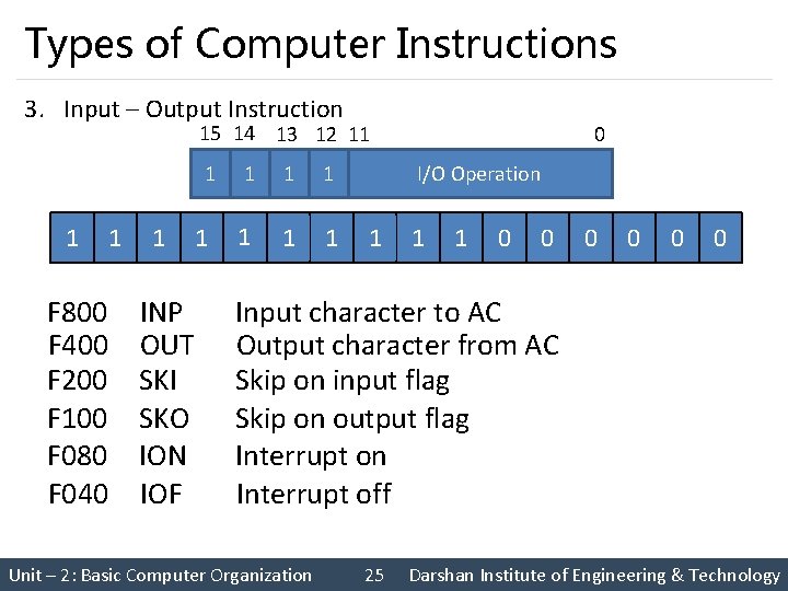
Types of Computer Instructions 3. Input – Output Instruction 15 14 13 12 11 1 1 F 800 F 400 F 200 F 100 F 080 F 040 1 1 INP OUT SKI SKO ION IOF 1 1 10 01 10 0 I/O Operation 01 1 0 0 0 0 Input character to AC Output character from AC Skip on input flag Skip on output flag Interrupt on Interrupt off Unit – 2: Basic Computer Organization 25 Darshan Institute of Engineering & Technology
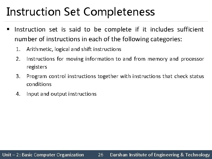
Instruction Set Completeness § Instruction set is said to be complete if it includes sufficient number of instructions in each of the following categories: 1. Arithmetic, logical and shift instructions 2. Instructions for moving information to and from memory and processor registers 3. Program control instructions together with instructions that check status conditions 4. Input and output instructions Unit – 2: Basic Computer Organization 26 Darshan Institute of Engineering & Technology
Timing & Control Unit – 2: Basic Computer Organization Darshan Institute of Engineering & Technology
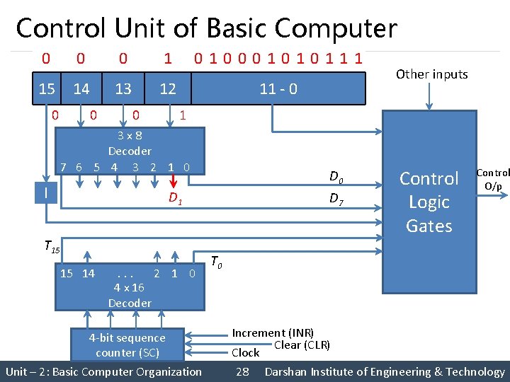
Control Unit of Basic Computer 0 0 0 Instruction Register 1 010001010111 15 14 13 0 0 12 0 11 ‐ 0 1 3 x 8 Decoder 7 6 5 4 3 2 1 0 I Other inputs D 0 D 1 T 15 15 14 . . . 2 1 0 4 x 16 Decoder 4‐bit sequence counter (SC) Unit – 2: Basic Computer Organization D 7 Control Logic Gates Control O/p T 0 Increment (INR) Clear (CLR) Clock 28 Darshan Institute of Engineering & Technology
Control Unit § Components of Control unit are 1. Two decoders 2. A sequence counter 3. Control logic gates § An instruction read from memory is placed in the instruction register (IR). § In control unit the IR is divided into three parts: I bit, the operation code (12‐ 14)bit, and bits 0 through 11. § The operation code in bits 12 through 14 are decoded with a 3 x 8 decoder. § Bit‐ 15 of the instruction is transferred to a flip‐flop designated by the symbol I. Unit – 2: Basic Computer Organization 29 Darshan Institute of Engineering & Technology
Control Unit § The eight outputs of the decoder are designated by the symbols D 0 through D 7. § Bits 0 through 11 are applied to the control logic gates. § The 4‐bit sequence counter can count in binary from 0 through 15. The outputs of counter are decoded into 16 timing signals T 0 through T 15. § The sequence counter SC can be incremented or cleared synchronously. § Most of the time, the counter is incremented to provide the sequence of timing signals out of 4 X 16 decoder. § Once in awhile, the counter is cleared to 0, causing the next timing signal to be T 0. Unit – 2: Basic Computer Organization 30 Darshan Institute of Engineering & Technology
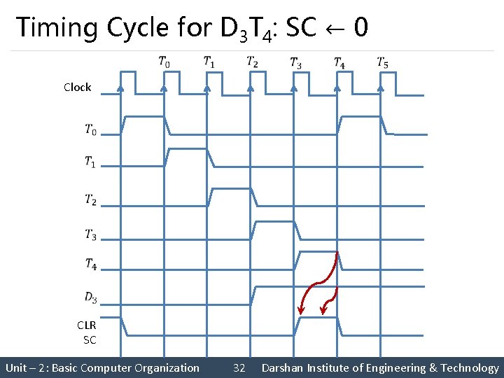
Control Unit § As an example, consider the case where SC is incremented to provide timing signals T 0, T 1, T 2, T 3 and T 4 in sequence. At time T 4, SC is cleared to 0 if decoder output D 3 is active. This is expressed symbolically by the statement D 3 T 4: SC ← 0 § Initially, the CLR input of SC is active. § The first positive transition of the clock clears SC to 0, which in turn activates the timing T 0 out of the decoder. § T 0 is active during one clock cycle. § The positive clock transition labeled T 0 in the diagram will trigger only those registers whose control inputs are connected to timing signal T 0. § SC is incremented with every positive clock transition, unless its CLR input is active. § This procedures the sequence of timing signals T 0, T 1, T 2, T 3 and T 4, and so on. If SC is not cleared, the timing signals will continue with T 5, T 6, up to T 15 and back to T 0. Unit – 2: Basic Computer Organization 31 Darshan Institute of Engineering & Technology
Timing Cycle for D 3 T 4: SC ← 0 Unit – 2: Basic Computer Organization 32 Clock CLR SC Darshan Institute of Engineering & Technology
Control Unit § The last three waveforms shows how SC is cleared when D 3 T 4 = 1. § Output D 3 from the operation decoder becomes active at the end of timing signal T 2. § When timing signal T 4 becomes active, the output of the AND gate that implements the control function D 3 T 4 becomes active. § This signal is applied to the CLR input of SC. § On the next positive clock transition the counter is cleared to 0. § This causes the timing signal T 0 to become active instead of T 5 that would have been active if SC were incremented instead of cleared. Unit – 2: Basic Computer Organization 33 Darshan Institute of Engineering & Technology
Control Organization § Hardwired Control • The control logic is implemented with gates, flips‐flops, decoders and other digital circuits. • It can be optimized to produce a fast mode of operation. • It requires changes in the wiring among the various components if the design has to be modified or changed. § Microprogrammed Control • The control information is stored in a control memory. • The control memory is programmed to initiate the required sequence of microoperations. • Any required changes or modifications can be done by updating the microprogram in control memory. Unit – 2: Basic Computer Organization 34 Darshan Institute of Engineering & Technology
Instruction Cycle § A program residing in the memory unit of the computer consists of a sequence of instructions. In the basic computer each instruction cycle consists of the following phases: 1. Fetch an instruction from memory. 2. Decode the instruction. 3. Read the effective address from memory if the instruction has an indirect address. 4. Execute the instruction. § After step 4, the control goes back to step 1 to fetch, decode and execute the next instruction. § This process continues unless a HALT instruction is encountered. Unit – 2: Basic Computer Organization 35 Darshan Institute of Engineering & Technology
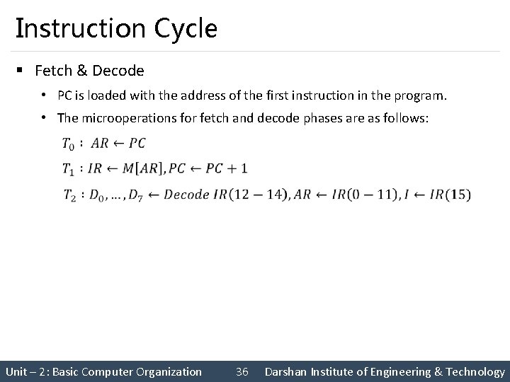
Instruction Cycle § Fetch & Decode • PC is loaded with the address of the first instruction in the program. • The microoperations for fetch and decode phases are as follows: Unit – 2: Basic Computer Organization 36 Darshan Institute of Engineering & Technology
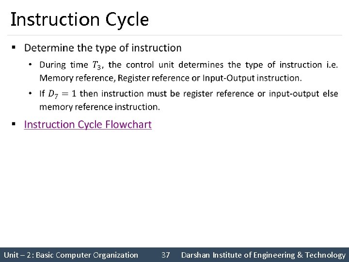
Instruction Cycle § Unit – 2: Basic Computer Organization 37 Darshan Institute of Engineering & Technology
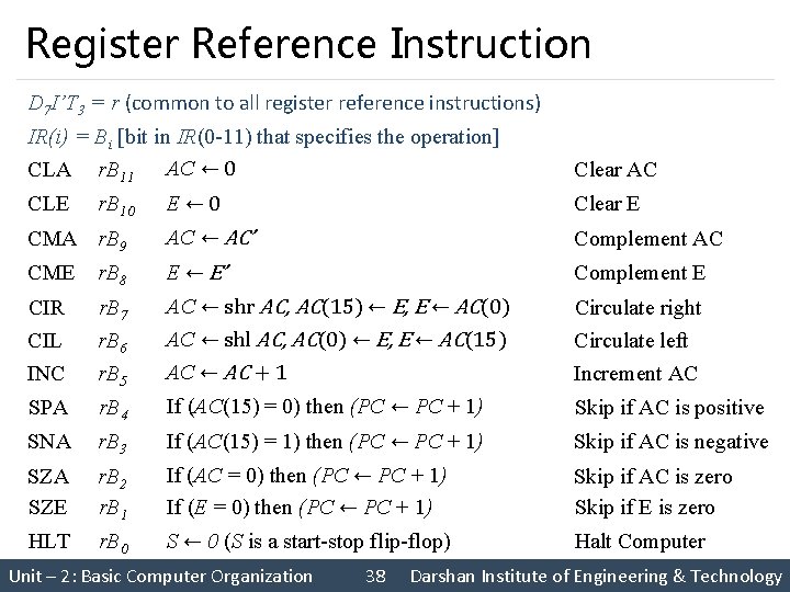
Register Reference Instruction D 7 I’T 3 = r (common to all register reference instructions) IR(i) = Bi [bit in IR(0 -11) that specifies the operation] CLA r. B 11 AC ← 0 Clear AC E← 0 Clear E CMA r. B 9 AC ← AC’ Complement AC CME r. B 8 E ← E’ Complement E CIR r. B 7 AC ← shr AC, AC(15) ← E, E ← AC(0) Circulate right CIL r. B 6 AC ← shl AC, AC(0) ← E, E ← AC(15) Circulate left INC r. B 5 AC ← AC + 1 Increment AC SPA r. B 4 If (AC(15) = 0) then (PC ← PC + 1) Skip if AC is positive SNA r. B 3 If (AC(15) = 1) then (PC ← PC + 1) Skip if AC is negative SZA SZE r. B 2 r. B 1 If (AC = 0) then (PC ← PC + 1) If (E = 0) then (PC ← PC + 1) Skip if AC is zero Skip if E is zero HLT r. B 0 S ← 0 (S is a start-stop flip-flop) Halt Computer CLE r. B 10 Unit – 2: Basic Computer Organization 38 Darshan Institute of Engineering & Technology
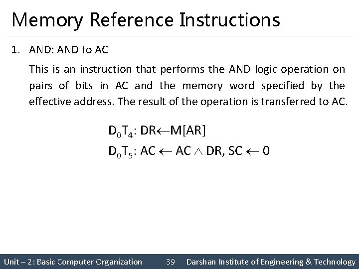
Memory Reference Instructions 1. AND: AND to AC This is an instruction that performs the AND logic operation on pairs of bits in AC and the memory word specified by the effective address. The result of the operation is transferred to AC. D 0 T 4: DR M[AR] D 0 T 5: AC DR, SC 0 Unit – 2: Basic Computer Organization 39 Darshan Institute of Engineering & Technology
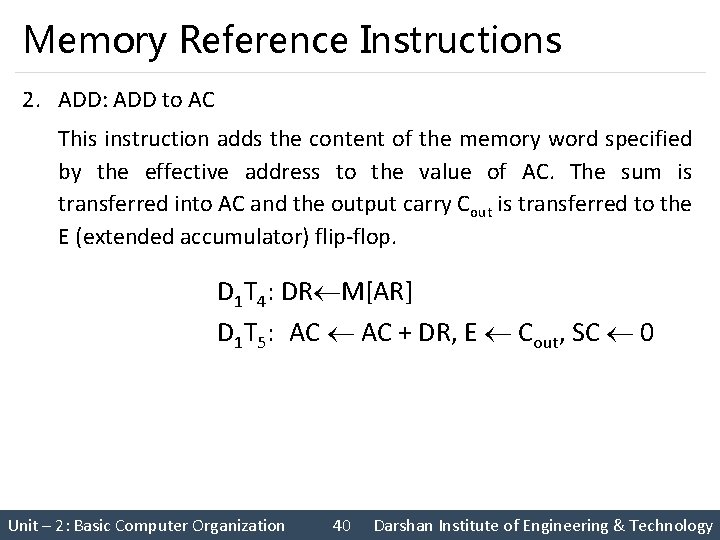
Memory Reference Instructions 2. ADD: ADD to AC This instruction adds the content of the memory word specified by the effective address to the value of AC. The sum is transferred into AC and the output carry Cout is transferred to the E (extended accumulator) flip‐flop. D 1 T 4: DR M[AR] D 1 T 5: AC + DR, E Cout, SC 0 Unit – 2: Basic Computer Organization 40 Darshan Institute of Engineering & Technology
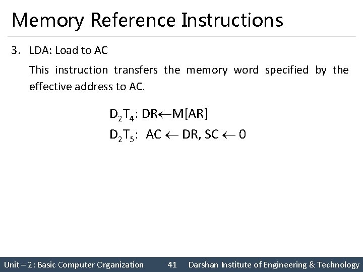
Memory Reference Instructions 3. LDA: Load to AC This instruction transfers the memory word specified by the effective address to AC. D 2 T 4: DR M[AR] D 2 T 5: AC DR, SC 0 Unit – 2: Basic Computer Organization 41 Darshan Institute of Engineering & Technology
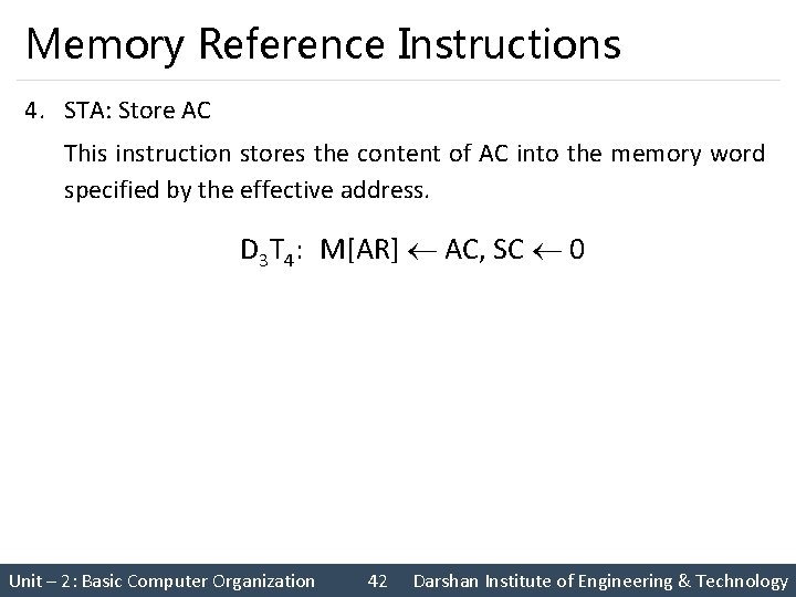
Memory Reference Instructions 4. STA: Store AC This instruction stores the content of AC into the memory word specified by the effective address. D 3 T 4: M[AR] AC, SC 0 Unit – 2: Basic Computer Organization 42 Darshan Institute of Engineering & Technology
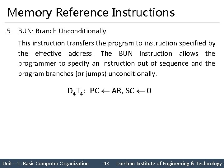
Memory Reference Instructions 5. BUN: Branch Unconditionally This instruction transfers the program to instruction specified by the effective address. The BUN instruction allows the programmer to specify an instruction out of sequence and the program branches (or jumps) unconditionally. D 4 T 4: PC AR, SC 0 Unit – 2: Basic Computer Organization 43 Darshan Institute of Engineering & Technology
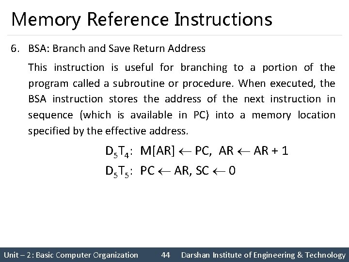
Memory Reference Instructions 6. BSA: Branch and Save Return Address This instruction is useful for branching to a portion of the program called a subroutine or procedure. When executed, the BSA instruction stores the address of the next instruction in sequence (which is available in PC) into a memory location specified by the effective address. D 5 T 4: M[AR] PC, AR + 1 D 5 T 5: PC AR, SC 0 Unit – 2: Basic Computer Organization 44 Darshan Institute of Engineering & Technology
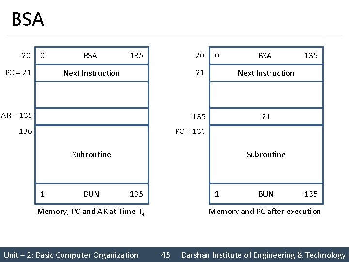
BSA 20 0 PC = 21 BSA 20 0 135 BSA 135 21 Next Instruction AR = 135 21 136 PC = 136 Next Instruction Subroutine 1 BUN Subroutine 135 1 Memory, PC and AR at Time T 4 Unit – 2: Basic Computer Organization BUN 135 Memory and PC after execution 45 Darshan Institute of Engineering & Technology
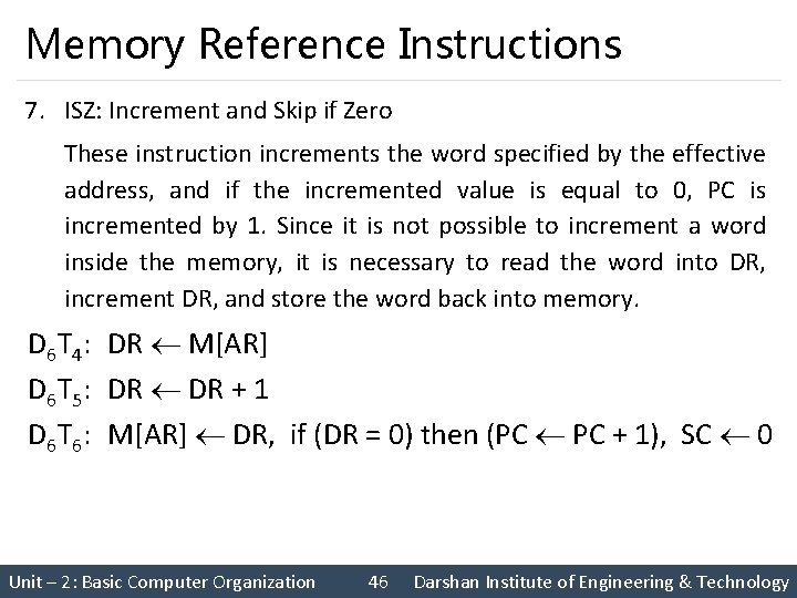
Memory Reference Instructions 7. ISZ: Increment and Skip if Zero These instruction increments the word specified by the effective address, and if the incremented value is equal to 0, PC is incremented by 1. Since it is not possible to increment a word inside the memory, it is necessary to read the word into DR, increment DR, and store the word back into memory. D 6 T 4: DR M[AR] D 6 T 5: DR + 1 D 6 T 6: M[AR] DR, if (DR = 0) then (PC PC + 1), SC 0 Unit – 2: Basic Computer Organization 46 Darshan Institute of Engineering & Technology
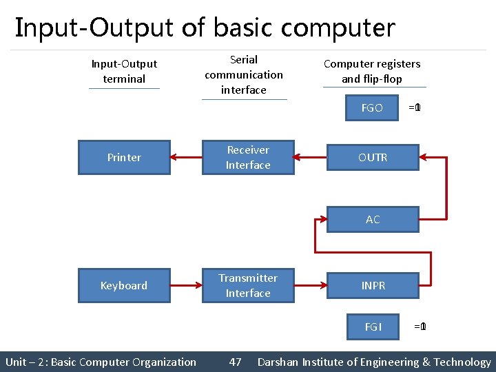
Input-Output of basic computer Input‐Output terminal Serial communication interface Computer registers and flip‐flop FGO Printer Receiver Interface =1 =0 OUTR AC Keyboard Transmitter Interface INPR FGI Unit – 2: Basic Computer Organization 47 =0 =1 Darshan Institute of Engineering & Technology
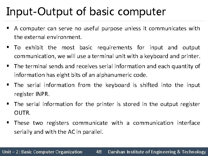
Input-Output of basic computer § A computer can serve no useful purpose unless it communicates with the external environment. § To exhibit the most basic requirements for input and output communication, we will use a terminal unit with a keyboard and printer. § The terminal sends and receives serial information and each quantity of information has eight bits of an alphanumeric code. § The serial information from the keyboard is shifted into the input register INPR. § The serial information for the printer is stored in the output register OUTR. § These two registers communicate with a communication interface serially and with the AC in parallel. Unit – 2: Basic Computer Organization 48 Darshan Institute of Engineering & Technology
Process of input information transfer § Initially, the input flag FGI is cleared to 0. When a key is struck in the keyboard, an 8‐bit alphanumeric code is shifted into INPR and the input flag FGI is set to 1. § As long as the flag is set, the information in INPR cannot be changed by striking another key. The computer checks the flag bit; if it is 1, the information from INPR is transferred in parallel into AC and FGI is cleared to 0. § Once the flag is cleared, new information can be shifted into INPR by striking another key. Unit – 2: Basic Computer Organization 49 Darshan Institute of Engineering & Technology
Process of outputting information § The output register OUTR works similarly but the direction of information flow is reversed. § Initially, the output flag FGO is set to 1. The computer checks the flag bit; if it is 1, the information from AC is transferred in parallel to OUTR and FGO is cleared to 0. The output device accepts the coded information, prints the corresponding character, and when the operation is completed, it sets FGO to 1. § The computer does not load a new character into OUTR when FGO is 0 because this condition indicates that the output device is in the process of printing the character. Unit – 2: Basic Computer Organization 50 Darshan Institute of Engineering & Technology
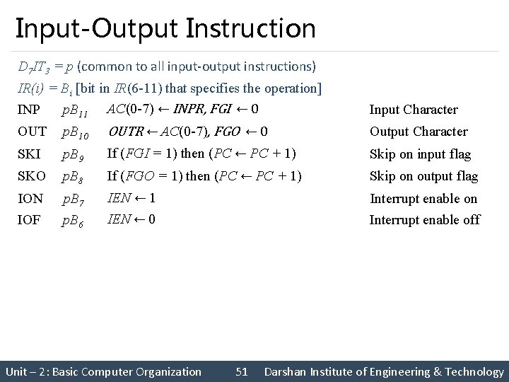
Input-Output Instruction D 7 IT 3 = p (common to all input‐output instructions) IR(i) = Bi [bit in IR(6 -11) that specifies the operation] INP p. B 11 AC(0 -7) ← INPR, FGI ← 0 Input Character OUT p. B 10 OUTR ← AC(0 -7), FGO ← 0 Output Character SKI p. B 9 If (FGI = 1) then (PC ← PC + 1) Skip on input flag SKO p. B 8 If (FGO = 1) then (PC ← PC + 1) Skip on output flag ION p. B 7 IEN ← 1 Interrupt enable on IOF p. B 6 IEN ← 0 Interrupt enable off Unit – 2: Basic Computer Organization 51 Darshan Institute of Engineering & Technology
![Interrupt Cycle Instruction cycle = 0 R Store return address in location 0 M[0] Interrupt Cycle Instruction cycle = 0 R Store return address in location 0 M[0]](http://slidetodoc.com/presentation_image/2fe21c1310a7b9dae58fc58fb6e1a1c3/image-52.jpg)
Interrupt Cycle Instruction cycle = 0 R Store return address in location 0 M[0] ← PC Fetch & Decode instruction Execute instruction IEN = 0 Branch to location 1 PC ← 1 = 1 FGI = 0 = 1 Interrupt cycle IEN ← 0 R ← 0 FGO = 0 R ← 1 Unit – 2: Basic Computer Organization 52 Darshan Institute of Engineering & Technology
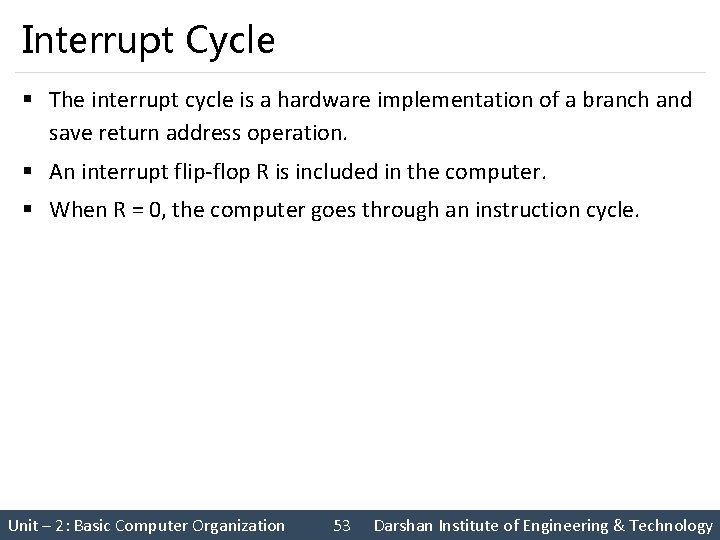
Interrupt Cycle § The interrupt cycle is a hardware implementation of a branch and save return address operation. § An interrupt flip‐flop R is included in the computer. § When R = 0, the computer goes through an instruction cycle. Unit – 2: Basic Computer Organization 53 Darshan Institute of Engineering & Technology
Interrupt Cycle § During the execute phase of the instruction cycle IEN is checked by the control. § If it is 0, it indicates that the programmer does not want to use the interrupt, so control continues with the next instruction cycle. § If IEN is 1, control checks the flag bits. § If both flags are 0, it indicates that neither the input nor the output registers are ready for transfer of information. § In this case, control continues with the next instruction cycle. If either flag is set to 1 while IEN = 1, flip‐flop R is set to 1. § At the end of the execute phase, control checks the value of R, and if it is equal to 1, it goes to an interrupt cycle instead of an instruction cycle. Unit – 2: Basic Computer Organization 54 Darshan Institute of Engineering & Technology
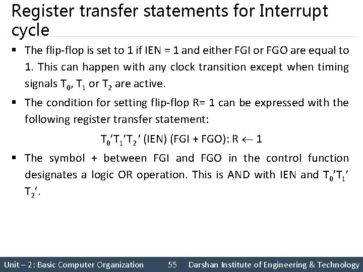
Register transfer statements for Interrupt cycle § The flip‐flop is set to 1 if IEN = 1 and either FGI or FGO are equal to 1. This can happen with any clock transition except when timing signals T 0, T 1 or T 2 are active. § The condition for setting flip‐flop R= 1 can be expressed with the following register transfer statement: T 0 T 1 T 2 (IEN) (FGI + FGO): R 1 § The symbol + between FGI and FGO in the control function designates a logic OR operation. This is AND with IEN and T 0 T 1 T 2. Unit – 2: Basic Computer Organization 55 Darshan Institute of Engineering & Technology
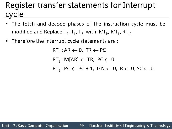
Register transfer statements for Interrupt cycle § The fetch and decode phases of the instruction cycle must be modified and Replace T 0, T 1, T 2 with R'T 0, R'T 1, R'T 2 § Therefore the interrupt cycle statements are : RT 0 : AR 0, TR PC RT 1 : M[AR] TR, PC 0 RT 2 : PC + 1, IEN 0, R 0, SC 0 Unit – 2: Basic Computer Organization 56 Darshan Institute of Engineering & Technology
Register transfer statements for Interrupt cycle § During the first timing signal AR is cleared to 0, and the content of PC is transferred to the temporary register TR. § With the second timing signal, the return address is stored in memory at location 0 and PC is cleared to 0. § The third timing signal increments PC to 1, clears IEN and R, and control goes back to T 0 by clearing SC to 0. § The beginning of the next instruction cycle has the condition RT 0 and the content of PC is equal to 1. The control then goes through an instruction cycle that fetches and executes the BUN instruction in location 1. Unit – 2: Basic Computer Organization 57 Darshan Institute of Engineering & Technology
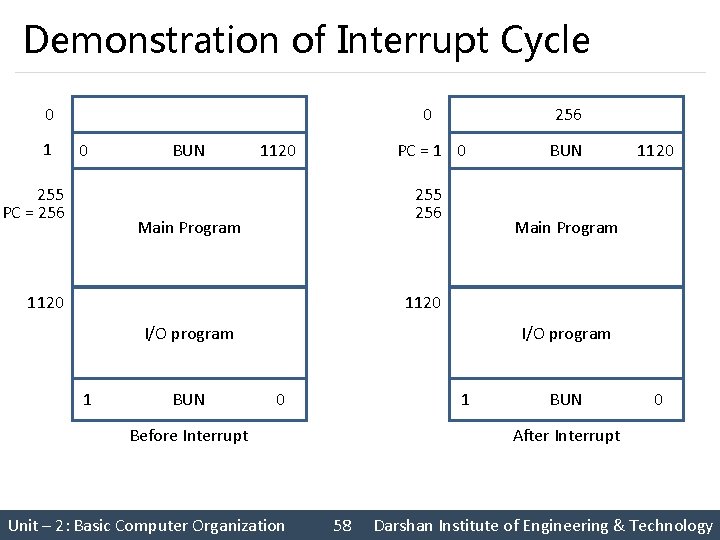
Demonstration of Interrupt Cycle 0 1 0 255 PC = 256 0 BUN 256 PC = 1 0 1120 255 256 Main Program 1120 BUN 1120 Main Program 1120 I/O program 1 BUN I/O program 0 1 Before Interrupt Unit – 2: Basic Computer Organization BUN 0 After Interrupt 58 Darshan Institute of Engineering & Technology
Design of Basic Computer § Basic Computer Unit – 2: Basic Computer Organization 59 Darshan Institute of Engineering & Technology
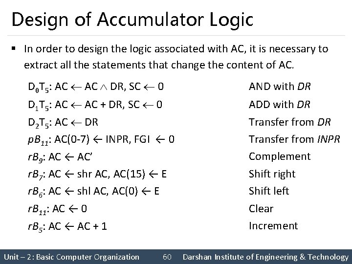
Design of Accumulator Logic § In order to design the logic associated with AC, it is necessary to extract all the statements that change the content of AC. D 0 T 5: AC DR, SC 0 AND with DR D 1 T 5: AC + DR, SC 0 D 2 T 5: AC DR p. B 11: AC(0‐ 7) ← INPR, FGI ← 0 r. B 9: AC ← AC’ r. B 7: AC ← shr AC, AC(15) ← E r. B 6: AC ← shl AC, AC(0) ← E r. B 11: AC ← 0 r. B 5: AC ← AC + 1 ADD with DR Transfer from INPR Complement Shift right Shift left Clear Increment Unit – 2: Basic Computer Organization 60 Darshan Institute of Engineering & Technology
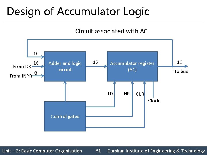
Design of Accumulator Logic Circuit associated with AC 16 From DR From INPR 16 8 Adder and logic circuit 16 Accumulator register (AC) LD INR 16 To bus CLR Clock Control gates Unit – 2: Basic Computer Organization 61 Darshan Institute of Engineering & Technology
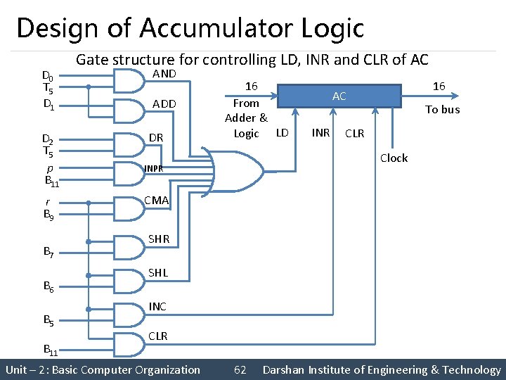
Design of Accumulator Logic D 0 T 5 D 1 D 2 T 5 p B 11 r B 9 B 7 B 6 B 5 B 11 Gate structure for controlling LD, INR and CLR of AC AND ADD DR 16 From Adder & Logic LD 16 AC INR To bus CLR Clock INPR CMA SHR SHL INC CLR Unit – 2: Basic Computer Organization 62 Darshan Institute of Engineering & Technology
Questions asked in GTU exam 1. Write a detailed note on instruction cycle with neat diagrams. 2. Explain control unit of basic computer and its working with diagram. 3. For the basic computer explain following instructions 1. 2. 3. 4. LDA ADD AND CLA 4. Draw and explain flowchart for interrupt cycle. 5. For the basic computer explain following instructions 1. 2. 3. 4. BUN BSA CIL SZE 6. Explain how Input/Output can be performed using interrupts. 7. State the differences between hardwired control and microprogrammed control. Unit – 2: Basic Computer Organization 63 Darshan Institute of Engineering & Technology
Questions asked in GTU exam 8. A computer uses a memory unit with 256 K words of 32 bits each. A binary instruction code is stored in one word of memory. The instruction has four parts: an indirect bit, an operation code, a register code part to specify one of 64 registers, and an address part. 1. How many bits are there in operation code, the register code part, and the address part? 2. Draw the instruction word format and indicate the number of bits in each part. 3. How many bits are there in the data and address inputs of the memory? 9. Draw and explain basic computer instruction formats. 10. Differentiate MRI and non‐MRI. 11. Memory reference instructions 12. Explain Direct and Indirect Addressing. 13. Give an example of register transfer of data through accumulator. 14. What is Interrupt? How it is useful for a system? 15. Explain CLA, ISZ, INP instruction. Unit – 2: Basic Computer Organization 64 Darshan Institute of Engineering & Technology
Questions asked in GTU exam 16. Explain with clear diagram, how data can be input to the computer using INP instruction. 17. What is a Program Counter? 18. What is an Accumulator? 19. What is an Instruction Register? 20. What do you understand by Memory Address? 21. What is a Carry Flag? 22. Explain Instruction Fetch. 23. Explain Instruction Decode. 24. Enlist major components of CPU. 25. Effective address Unit – 2: Basic Computer Organization 65 Darshan Institute of Engineering & Technology
- Slides: 65