2011 1 Special Topics in Optical Communications Optical

- Slides: 19

2011 -1 Special Topics in Optical Communications Optical Interconnects: Out of the Box Forever? Dawei Huang, IEEE Journal of Selected Topics in Quantum Electronics, March/April 2003 Jeong-Min Lee (minlj@tera. yonsei. ac. kr) High-Speed Circuits and Systems LAB.

2011 -1 Special Topics in Optical Communications Contents 1. Introduction 2. Computer Design (A ~ D) 3. Electrical and Optical Interconnects (A ~ F) 4. Scaling into the Future High-Speed Circuits and Systems LAB. 2

2011 -1 Special Topics in Optical Communications Introduction § Recent research: Optical interconnects are a viable alternative electrical interconnects for board-to-board, chip-to-chip, and on-chip application § Overview of the performance scaling that has driven current computer design focus on architectural design and effects of these designs on interconnect implementation § Optical interconnects outperform electrical interconnects for longdistance applications § Advantages of optical interconnects: time of flight & BW density § Characterize what would be required for optical interconnects to displace wires at the backplane, board, and chip level. High-Speed Circuits and Systems LAB. 3

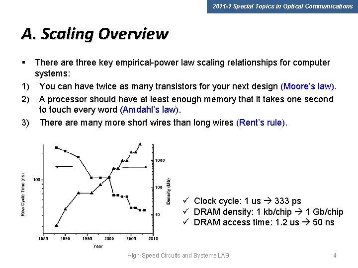
2011 -1 Special Topics in Optical Communications A. Scaling Overview § There are three key empirical-power law scaling relationships for computer systems: 1) You can have twice as many transistors for your next design (Moore’s law). 2) A processor should have at least enough memory that it takes one second to touch every word (Amdahl’s law). 3) There are many more short wires than long wires (Rent’s rule). ü Clock cycle: 1 us 333 ps ü DRAM density: 1 kb/chip 1 Gb/chip ü DRAM access time: 1. 2 us 50 ns High-Speed Circuits and Systems LAB. 4

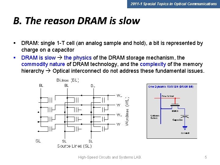
2011 -1 Special Topics in Optical Communications B. The reason DRAM is slow § § DRAM: single 1 -T cell (an analog sample and hold), a bit is represented by charge on a capacitor DRAM is slow the physics of the DRAM storage mechanism, the commodity nature of DRAM technology, and the complexity of the memory hierarchy Optical interconnect do not address these fundamental issues. High-Speed Circuits and Systems LAB. 5

2011 -1 Special Topics in Optical Communications B. The reason DRAM is slow § The maximum number of bits per bit line is limited by the ratio Capacitance: storage node, bit line, input stage of the sense amplifier § When the charge in the storage capacitor is gated onto the bit line, the charge spreads by RC-limited diffusion, which results in access time depending on (the number of bits per bit line)2. § In summary, DRAM latency is a significant design constraint, limited by the device design optimization. Optical interconnects cannot solve this DRAM access problem. High-Speed Circuits and Systems LAB. 6

2011 -1 Special Topics in Optical Communications C. Simple Machines § § § Optical interconnects has focused on tradeoffs between bandwidth, power, circuit area, and signal integrity. A large fraction of the work done by a computer merely produces memory addresses and moves bits back and forth. 4 memory accesses: one to fetch the instruction, two to fetch the operands, and one to write back the result. Cache: a small fast memory between the process & main memory A cache retains copies of recently fetched memory locations. If the processor should request a value already present in the cache, the local copy is quickly delivered and latency is reduced. High-Speed Circuits and Systems LAB. 7

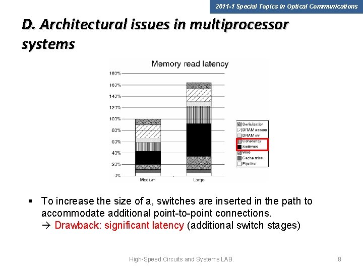
2011 -1 Special Topics in Optical Communications D. Architectural issues in multiprocessor systems § To increase the size of a, switches are inserted in the path to accommodate additional point-to-point connections. Drawback: significant latency (additional switch stages) High-Speed Circuits and Systems LAB. 8

2011 -1 Special Topics in Optical Communications D. Architectural issues in multiprocessor systems § Optical interconnects at the backplane level higher density optical input/output (I/O) can be provided to a switch chip reduction in the number of switch stages reduce latency in large servers § Cache coherence protocol: significant factor for memory latency When large caches are placed close to each processor significant fraction of memory accesses can be satisfied with data from other processors’ caches, rather than from main memory High-Speed Circuits and Systems LAB. 9

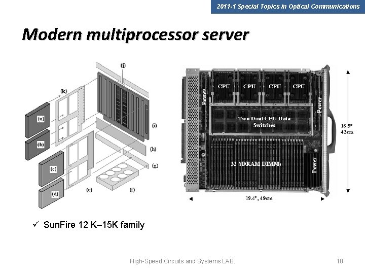
2011 -1 Special Topics in Optical Communications Modern multiprocessor server ü Sun. Fire 12 K– 15 K family High-Speed Circuits and Systems LAB. 10

2011 -1 Special Topics in Optical Communications A. Circuit board wiring density § Two factors control the wiring density on a circuit board the pitch of the signal lines & via construction § The via holes may block half the available space for wiring on every layer of the board Additional wiring layers is required to make routing possible. § Alternative methods forming vias ① Laminate boards may incorporate buried or blind vias (more expensive than conventional boards, because of lower yield) ② One alternative to laminated circuit boards is multilayer ceramic circuit boards available with alumina and low temperature glass–ceramic bodies. High-Speed Circuits and Systems LAB. 11

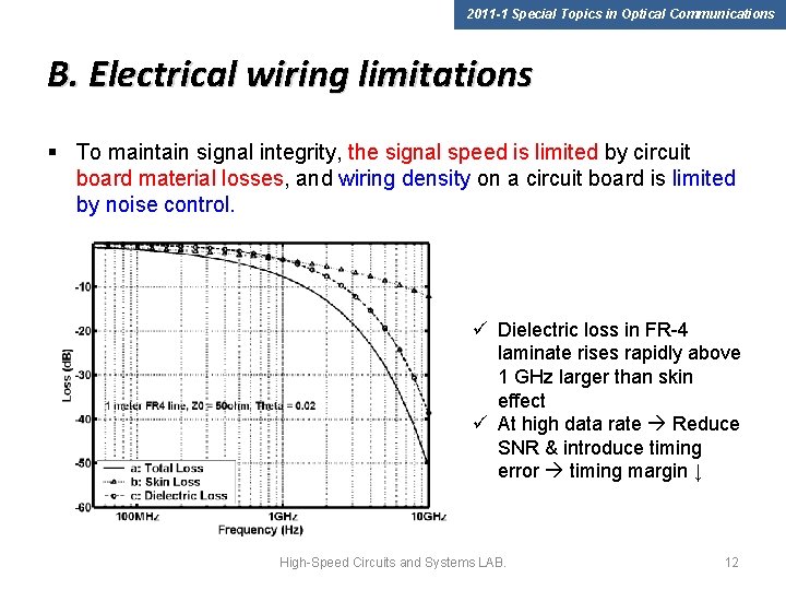
2011 -1 Special Topics in Optical Communications B. Electrical wiring limitations § To maintain signal integrity, the signal speed is limited by circuit board material losses, and wiring density on a circuit board is limited by noise control. ü Dielectric loss in FR-4 laminate rises rapidly above 1 GHz larger than skin effect ü At high data rate Reduce SNR & introduce timing error timing margin ↓ High-Speed Circuits and Systems LAB. 12

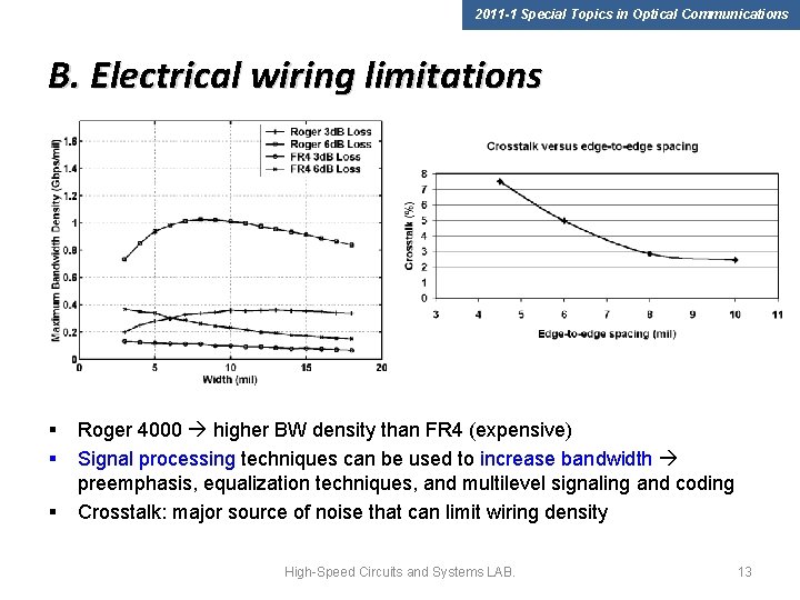
2011 -1 Special Topics in Optical Communications B. Electrical wiring limitations § § § Roger 4000 higher BW density than FR 4 (expensive) Signal processing techniques can be used to increase bandwidth preemphasis, equalization techniques, and multilevel signaling and coding Crosstalk: major source of noise that can limit wiring density High-Speed Circuits and Systems LAB. 13

2011 -1 Special Topics in Optical Communications C. Bandwidth density to memory § While the use of optical interconnects will not help with memory access latency significantly help to relieve wiring congestion to memory. § DIMM socket produce a difficult routing situation under the sockets to route each memory connector contact to the memory controller spread out on multiple layers § Using optics instead of a circuit board free-space optical system would not have wiring congestion problems. (require adding optical I/O to each DIMM) High-Speed Circuits and Systems LAB. 14

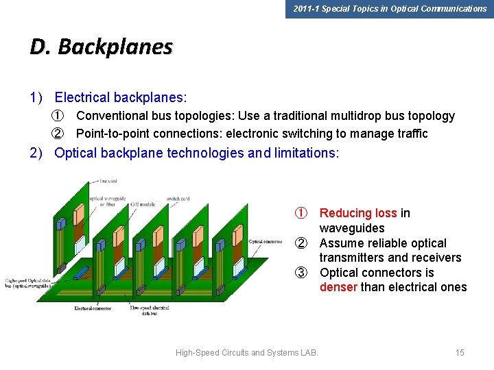
2011 -1 Special Topics in Optical Communications D. Backplanes 1) Electrical backplanes: ① Conventional bus topologies: Use a traditional multidrop bus topology ② Point-to-point connections: electronic switching to manage traffic 2) Optical backplane technologies and limitations: ① Reducing loss in waveguides ② Assume reliable optical transmitters and receivers ③ Optical connectors is denser than electrical ones High-Speed Circuits and Systems LAB. 15

2011 -1 Special Topics in Optical Communications D. Backplanes 3) Optical backplane technology disruption: – Freedom from wiring congestion In exchange for the optical components part of the backplane multiple routing chips and some protocol overhead could be eliminated. – An example of a unique optical solution is global clock distribution in backplane design. High-Speed Circuits and Systems LAB. 16

2011 -1 Special Topics in Optical Communications E. Chip-to-chip connection § Processor chip: 5000 connections power (2/3) + high speed signal ① The processor is mounted face down in a package transforms the 0. 25 -mm typical pitch of the solder ball connections on the chip ② Several processors, switches, and cache memory will be located on a single multilayer ceramic circuit board § Alignment of the ICs to the optical system remains an open issue. ① Multimode fiber passive alignment ② Single-mode fiber active alignment § The materials used for supporting an array of chips that are optically interconnected must be selected very carefully Thermal expansion & residual stress § Important consideration is the operating temperature of the optical devices (VCSEL: temperature sensitivity) High-Speed Circuits and Systems LAB. 17

2011 -1 Special Topics in Optical Communications F. On-chip wiring 1) Local vs. Global ü ü ü 2) RC or resistance-inductance-capacitance propagation mode ü ü 3) Local wire: connect TR to gates, lithography resolution Global wire: connect functions across the chip, edge length of the chip Thickness of both wire & dielectric layers controlled by deposition technology (~1 um) RC time improved with the (lithographic scaling)2 C: conductor dimension, dielectric constant, short wire cap ↓ R: ratio of length to cross section (W, t lithography dimension) Al Cu: less resistance Optical interconnect: wiring, clock distribution ü Potential of carrying very high-frequency signal High-Speed Circuits and Systems LAB. 18

2011 -1 Special Topics in Optical Communications Scaling into the future § In order for the pricing of optical backplanes to become competitive with electrical alternatives standard would need to be established. § Memory: latency is due to the speed of the DRAM component itself, and not due to time of flight limitations Little that optics can do to speed up access to memory § Chip-to-chip optical communication is the easiest of the short distance applications § Recent work on photonic bandgap materials has renewed interest in hybrid optical-electrical interconnects at this scale, High-Speed Circuits and Systems LAB. 19