2 Reciprocal Lattice Issues that are addressed in
- Slides: 13

2. Reciprocal Lattice Issues that are addressed in this chapter include: Ø Ø Bragg law Scattered wave amplitude Brillouin Zones Fourier analysis of the basis EEE 539 Solid State Electronics

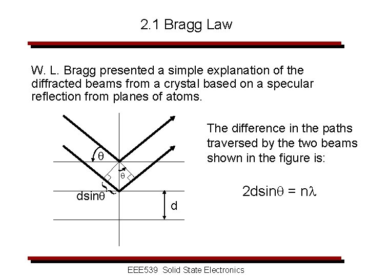
2. 1 Bragg Law W. L. Bragg presented a simple explanation of the diffracted beams from a crystal based on a specular reflection from planes of atoms. The difference in the paths traversed by the two beams shown in the figure is: { dsin d 2 dsin = nl EEE 539 Solid State Electronics

Listed below are some additional notes on the Bragg reflection: ¥ Although the reflection from each plane is specular, only for certain values of will the reflections from all planes add up in phase to give a strong reflected beam. ¥ Each plane reflects only 10 -3 to 10 -5 of the incident radiation, i. e. it is not a perfect reflector. Hence, 103 to 105 planes contribute to the formation of the Bragg-reflected beam in a perfect crystal. ¥ The composition of the basis determines the relative intensity of the various orders of diffraction. EEE 539 Solid State Electronics

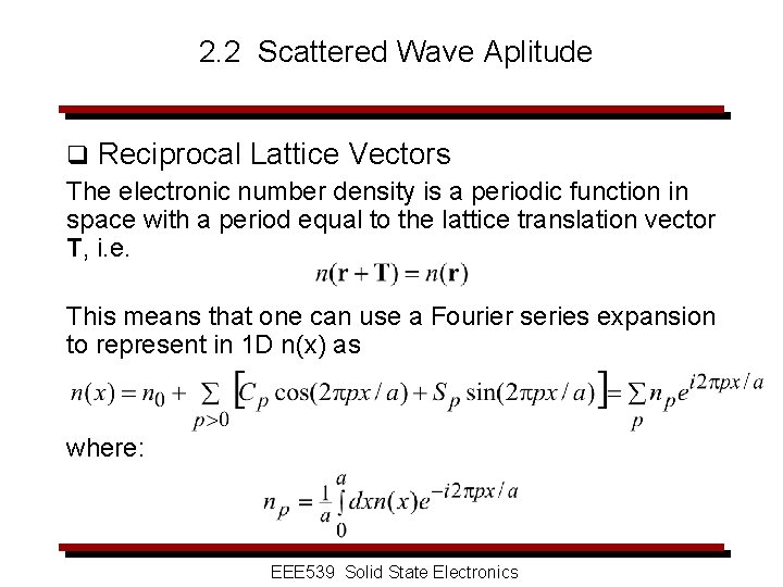
2. 2 Scattered Wave Aplitude q Reciprocal Lattice Vectors The electronic number density is a periodic function in space with a period equal to the lattice translation vector T, i. e. This means that one can use a Fourier series expansion to represent in 1 D n(x) as where: EEE 539 Solid State Electronics

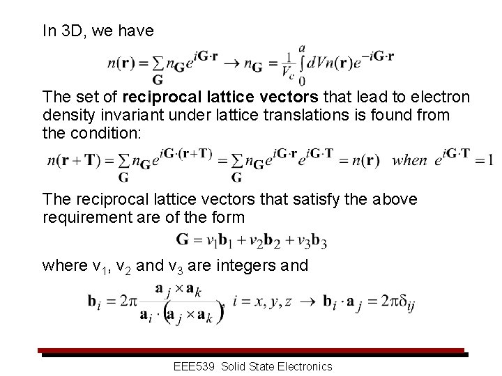
In 3 D, we have The set of reciprocal lattice vectors that lead to electron density invariant under lattice translations is found from the condition: The reciprocal lattice vectors that satisfy the above requirement are of the form where v 1, v 2 and v 3 are integers and EEE 539 Solid State Electronics

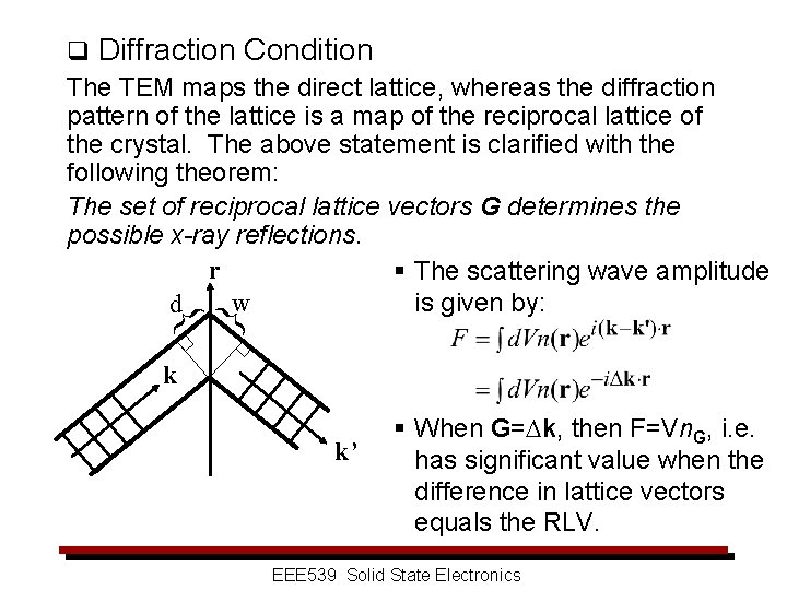
{ { q Diffraction Condition The TEM maps the direct lattice, whereas the diffraction pattern of the lattice is a map of the reciprocal lattice of the crystal. The above statement is clarified with the following theorem: The set of reciprocal lattice vectors G determines the possible x-ray reflections. r § The scattering wave amplitude w is given by: d k k’ § When G=Dk, then F=Vn. G, i. e. has significant value when the difference in lattice vectors equals the RLV. EEE 539 Solid State Electronics

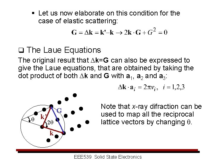
§ Let us now elaborate on this condition for the case of elastic scattering: q The Laue Equations The original result that Dk=G can also be expressed to give the Laue equations, that are obtained by taking the dot product of both Dk and G with a 1, a 2 and a 3: k’ G 2 Note that x-ray difraction can be used to map all the reciprocal lattice vectors by changing . k EEE 539 Solid State Electronics

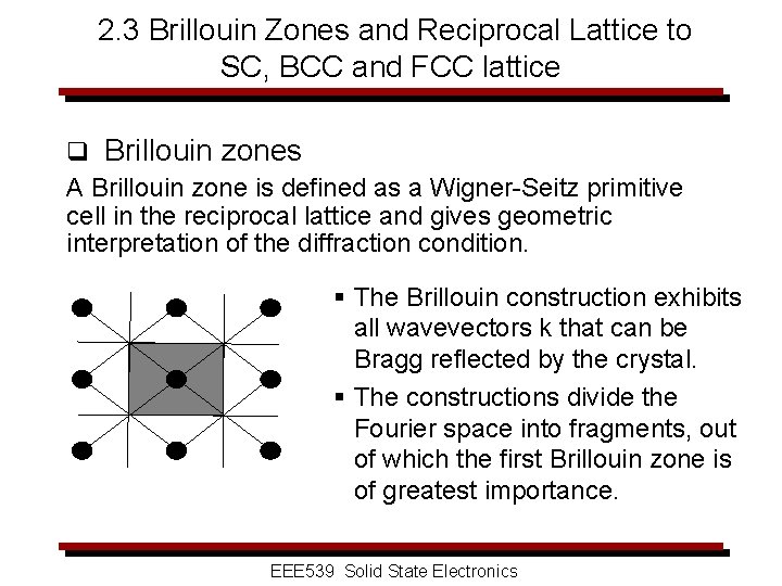
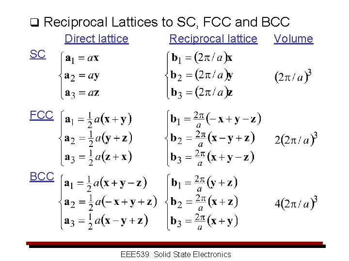
2. 3 Brillouin Zones and Reciprocal Lattice to SC, BCC and FCC lattice q Brillouin zones A Brillouin zone is defined as a Wigner-Seitz primitive cell in the reciprocal lattice and gives geometric interpretation of the diffraction condition. § The Brillouin construction exhibits all wavevectors k that can be Bragg reflected by the crystal. § The constructions divide the Fourier space into fragments, out of which the first Brillouin zone is of greatest importance. EEE 539 Solid State Electronics

q Reciprocal Lattices to SC, FCC and BCC Direct lattice Reciprocal lattice Volume SC FCC BCC EEE 539 Solid State Electronics

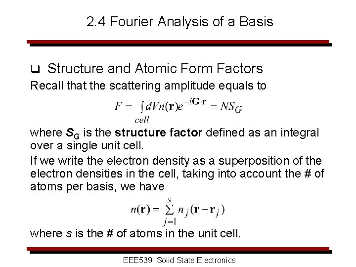
2. 4 Fourier Analysis of a Basis q Structure and Atomic Form Factors Recall that the scattering amplitude equals to where SG is the structure factor defined as an integral over a single unit cell. If we write the electron density as a superposition of the electron densities in the cell, taking into account the # of atoms per basis, we have where s is the # of atoms in the unit cell. EEE 539 Solid State Electronics

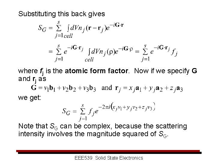
Substituting this back gives where fj is the atomic form factor. Now if we specify G and rj as we get: Note that SG can be complex, because the scattering intensity involves the magnitude squared of SG. EEE 539 Solid State Electronics

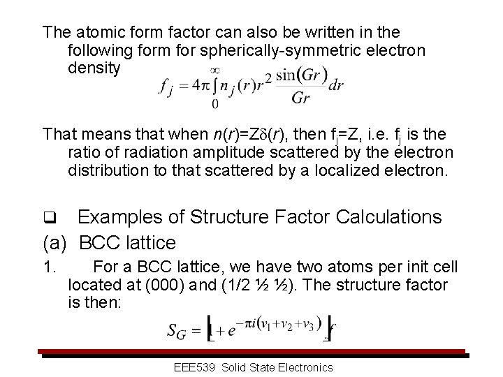
The atomic form factor can also be written in the following form for spherically-symmetric electron density That means that when n(r)=Zd(r), then fj=Z, i. e. fj is the ratio of radiation amplitude scattered by the electron distribution to that scattered by a localized electron. Examples of Structure Factor Calculations (a) BCC lattice q 1. For a BCC lattice, we have two atoms per init cell located at (000) and (1/2 ½ ½). The structure factor is then: EEE 539 Solid State Electronics

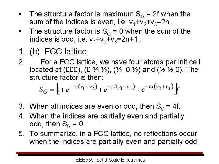
§ § The structure factor is maximum SG = 2 f when the sum of the indices is even, i. e. v 1+v 2+v 3=2 n. The structure factor is SG = 0 when the sum of the indices is odd, i. e. v 1+v 2+v 3=2 n+1. 1. (b) FCC lattice 2. For a FCC lattice, we have four atoms per init cell located at (000), (0 ½ ½), (½ 0 ½) and (½ ½ 0). The structure factor is then: 3. When all indices are even or odd, then SG = 4 f. 4. When the indices are partially even and partially odd, then SG = 0. 5. To summarize, in a FCC lattice, no reflections occur when the indices are partially even and partially odd. EEE 539 Solid State Electronics