2 D Plasmonic Imaging For Optical Lithography Josh
- Slides: 8

2 -D Plasmonic Imaging For Optical Lithography Josh Conway Prof. Eli Yablonovitch Opto-Electronics Group Electrical Engineering Department UCLA MURI Review Meeting, October 2003

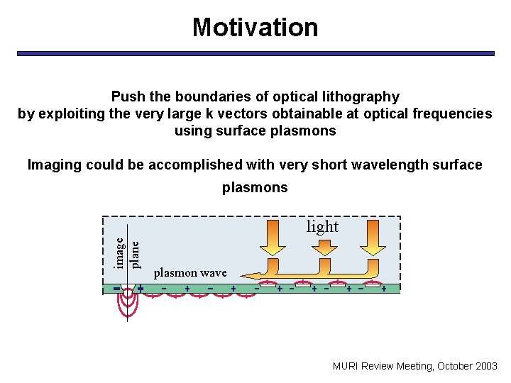
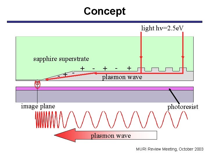
Motivation Push the boundaries of optical lithography by exploiting the very large k vectors obtainable at optical frequencies using surface plasmons Imaging could be accomplished with very short wavelength surface plasmons image plane light plasmon wave MURI Review Meeting, October 2003

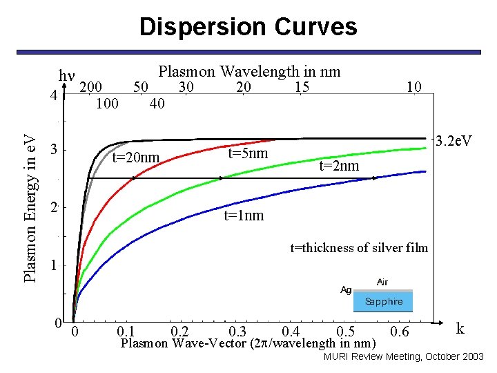
Dispersion Curves h Plasmon Energy in e. V 4 3 Plasmon Wavelength in nm 200 50 30 100 40 20 15 3. 2 e. V t=5 nm t=20 nm 2 10 t=2 nm t=1 nm t=thickness of silver film 1 0 0 0. 1 0. 2 0. 3 0. 4 0. 5 Plasmon Wave-Vector (2 /wavelength in nm) 0. 6 k MURI Review Meeting, October 2003

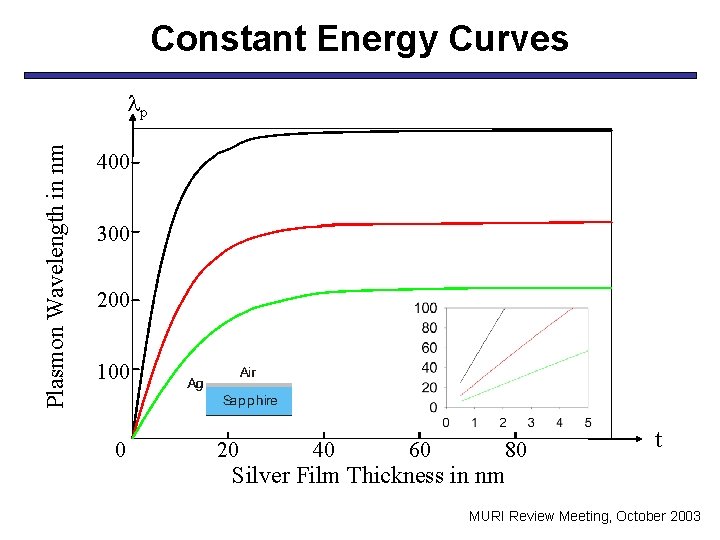
Constant Energy Curves Plasmon Wavelength in nm p 400 300 200 100 0 20 40 60 80 t Silver Film Thickness in nm MURI Review Meeting, October 2003

Concept light h =2. 5 e. V sapphire superstrate + - + - + plasmon wave image plane photoresist plasmon wave MURI Review Meeting, October 2003

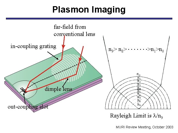
Plasmon Imaging far-field from conventional lens in-coupling grating n 9> n 8> >n 1>n 0 dimple lens out-coupling slot Rayleigh Limit is /n 9 MURI Review Meeting, October 2003

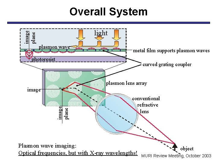
image plane Overall System light plasmon wave metal film supports plasmon waves photoresist curved grating coupler plasmon lens array image plane image conventional refractive lens Plasmon wave imaging: Optical frequencies, but with X-ray wavelengths! object MURI Review Meeting, October 2003

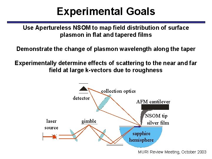
Experimental Goals Use Apertureless NSOM to map field distribution of surface plasmon in flat and tapered films Demonstrate the change of plasmon wavelength along the taper Experimentally determine effects of scattering to the near and far field at large k-vectors due to roughness collection optics detector laser source gimble AFM cantilever NSOM tip silver film sapphire hemisphere MURI Review Meeting, October 2003