2 1 2 RS 485 Data Interface RS
- Slides: 69

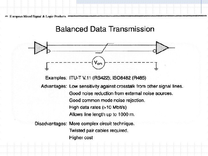
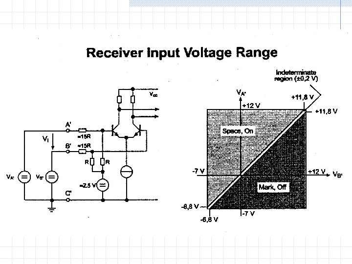
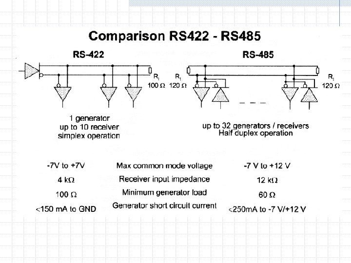
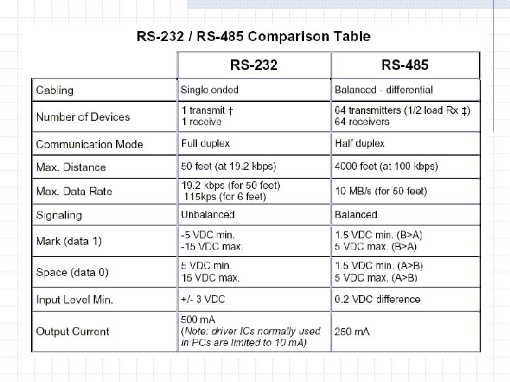
2. 1. 2 RS 485 Data Interface RS 485 AC, DC, & PIN power RS 485 Fiber & Copper Modem RS 485 Telephone modems RS 485 converter RS 485 opto isolation RS 485 drivers RS 485 Data Acquisition Communications


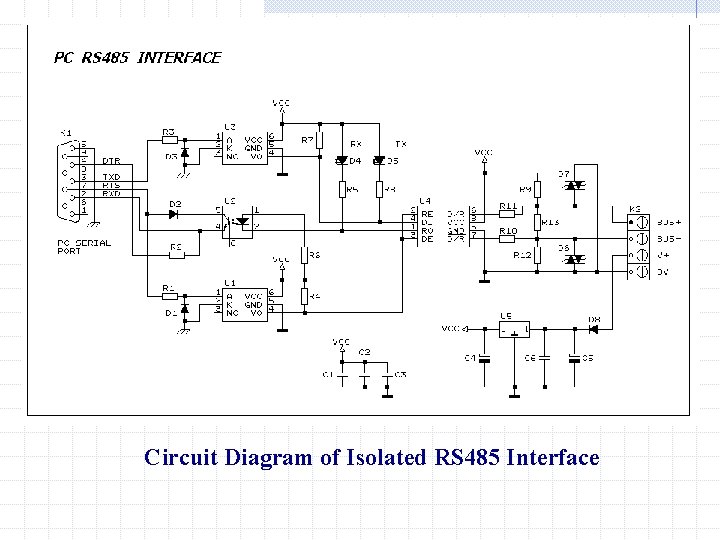
Circuit Diagram of Isolated RS 485 Interface

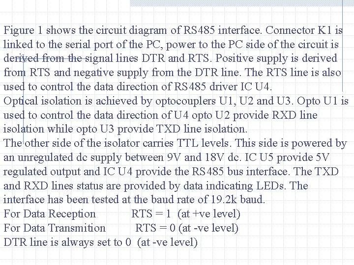
Figure 1 shows the circuit diagram of RS 485 interface. Connector K 1 is linked to the serial port of the PC, power to the PC side of the circuit is derived from the signal lines DTR and RTS. Positive supply is derived from RTS and negative supply from the DTR line. The RTS line is also used to control the data direction of RS 485 driver IC U 4. Optical isolation is achieved by optocouplers U 1, U 2 and U 3. Opto U 1 is used to control the data direction of U 4 opto U 2 provide RXD line isolation while opto U 3 provide TXD line isolation. The other side of the isolator carries TTL levels. This side is powered by an unregulated dc supply between 9 V and 18 V dc. IC U 5 provide 5 V regulated output and IC U 4 provide the RS 485 bus interface. The TXD and RXD lines status are provided by data indicating LEDs. The interface has been tested at the baud rate of 19. 2 k baud. For Data Reception RTS = 1 (at +ve level) For Data Transmition RTS = 0 (at -ve level) DTR line is always set to 0 (at -ve level)

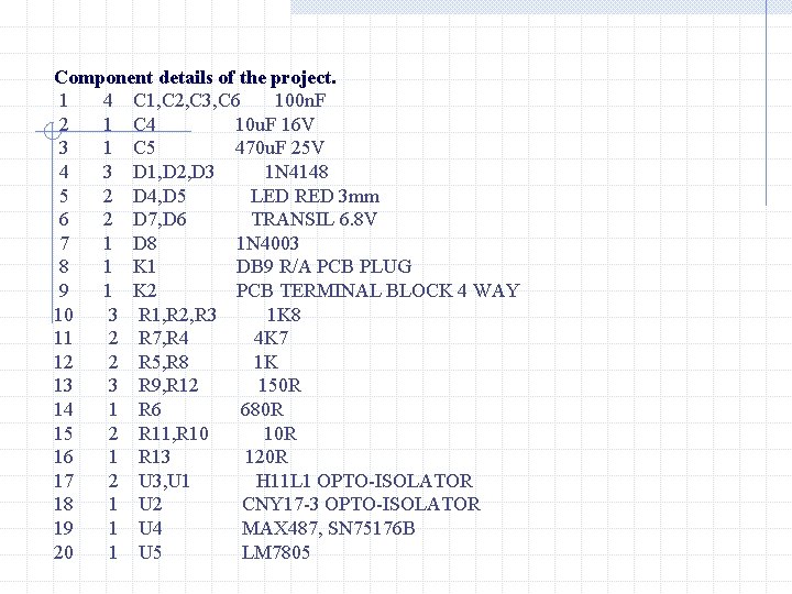
Component details of the project. 1 4 C 1, C 2, C 3, C 6 100 n. F 2 1 C 4 10 u. F 16 V 3 1 C 5 470 u. F 25 V 4 3 D 1, D 2, D 3 1 N 4148 5 2 D 4, D 5 LED RED 3 mm 6 2 D 7, D 6 TRANSIL 6. 8 V 7 1 D 8 1 N 4003 8 1 K 1 DB 9 R/A PCB PLUG 9 1 K 2 PCB TERMINAL BLOCK 4 WAY 10 3 R 1, R 2, R 3 1 K 8 11 2 R 7, R 4 4 K 7 12 2 R 5, R 8 1 K 13 3 R 9, R 12 150 R 14 1 R 6 680 R 15 2 R 11, R 10 10 R 16 1 R 13 120 R 17 2 U 3, U 1 H 11 L 1 OPTO-ISOLATOR 18 1 U 2 CNY 17 -3 OPTO-ISOLATOR 19 1 U 4 MAX 487, SN 75176 B 20 1 U 5 LM 7805

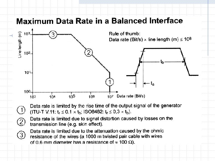
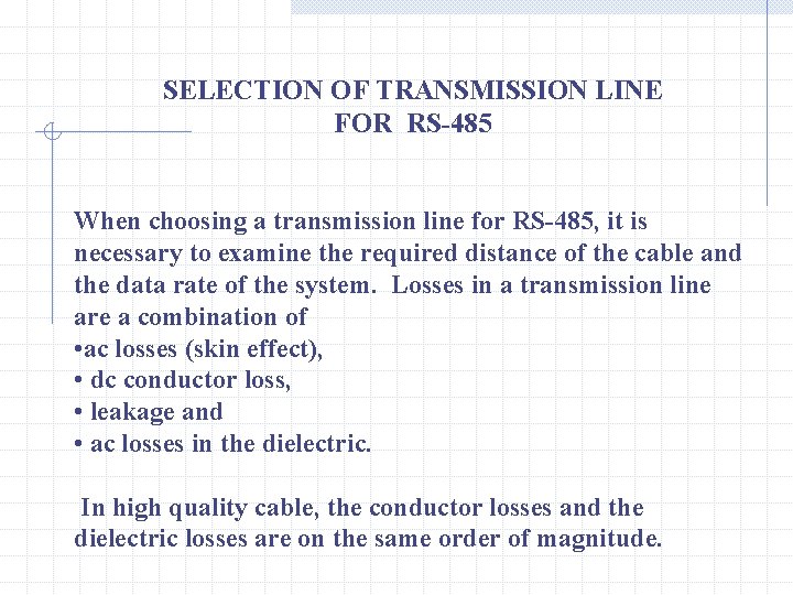
SELECTION OF TRANSMISSION LINE FOR RS-485 When choosing a transmission line for RS-485, it is necessary to examine the required distance of the cable and the data rate of the system. Losses in a transmission line are a combination of • ac losses (skin effect), • dc conductor loss, • leakage and • ac losses in the dielectric. In high quality cable, the conductor losses and the dielectric losses are on the same order of magnitude.

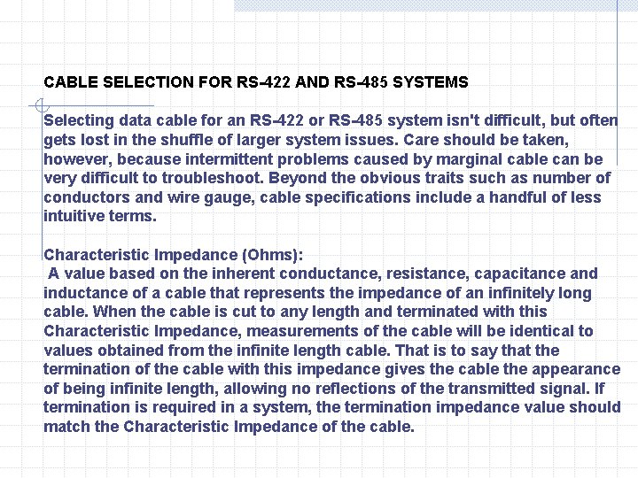
CABLE SELECTION FOR RS-422 AND RS-485 SYSTEMS Selecting data cable for an RS-422 or RS-485 system isn't difficult, but often gets lost in the shuffle of larger system issues. Care should be taken, however, because intermittent problems caused by marginal cable can be very difficult to troubleshoot. Beyond the obvious traits such as number of conductors and wire gauge, cable specifications include a handful of less intuitive terms. Characteristic Impedance (Ohms): A value based on the inherent conductance, resistance, capacitance and inductance of a cable that represents the impedance of an infinitely long cable. When the cable is cut to any length and terminated with this Characteristic Impedance, measurements of the cable will be identical to values obtained from the infinite length cable. That is to say that the termination of the cable with this impedance gives the cable the appearance of being infinite length, allowing no reflections of the transmitted signal. If termination is required in a system, the termination impedance value should match the Characteristic Impedance of the cable.

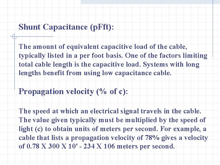
Shunt Capacitance (p. Fft): The amount of equivalent capacitive load of the cable, typically listed in a per foot basis. One of the factors limiting total cable length is the capacitive load. Systems with long lengths benefit from using low capacitance cable. Propagation velocity (% of c): The speed at which an electrical signal travels in the cable. The value given typically must be multiplied by the speed of light (c) to obtain units of meters per second. For example, a cable that lists a propagation velocity of 78% gives a velocity of 0. 78 X 300 X 10' - 234 X 106 meters per second.

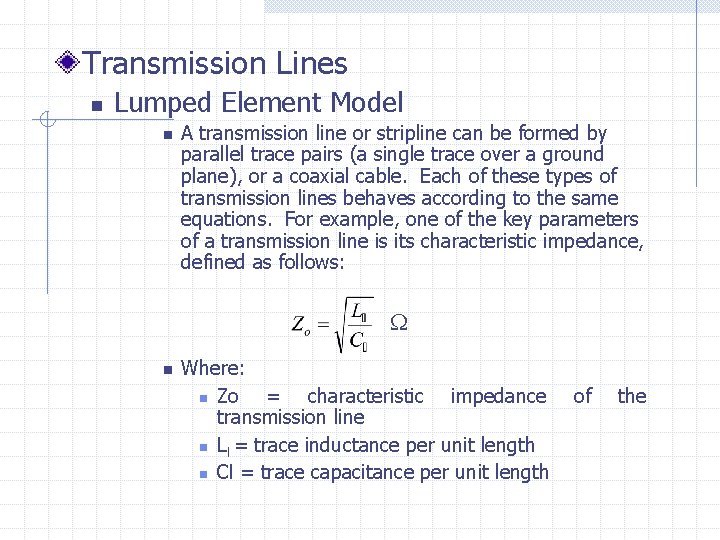
Transmission Lines n Lumped Element Model n A transmission line or stripline can be formed by parallel trace pairs (a single trace over a ground plane), or a coaxial cable. Each of these types of transmission lines behaves according to the same equations. For example, one of the key parameters of a transmission line is its characteristic impedance, defined as follows: n Where: n Zo = characteristic impedance transmission line n Ll = trace inductance per unit length n Cl = trace capacitance per unit length of the

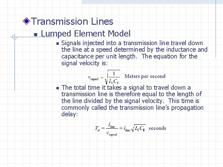
Transmission Lines n Lumped Element Model n Signals injected into a transmission line travel down the line at a speed determined by the inductance and capacitance per unit length. The equation for the signal velocity is: Meters per second n The total time it takes a signal to travel down a transmission line is therefore equal to the length of the line divided by the signal velocity. This time is commonly called the transmission line’s propagation delay: seconds

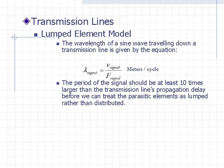
Transmission Lines n Lumped Element Model n The wavelength of a sine wave travelling down a transmission line is given by the equation: Meters / cycle n The period of the signal should be at least 10 times larger than the transmission line’s propagation delay before we can treat the parasitic elements as lumped rather than distributed.

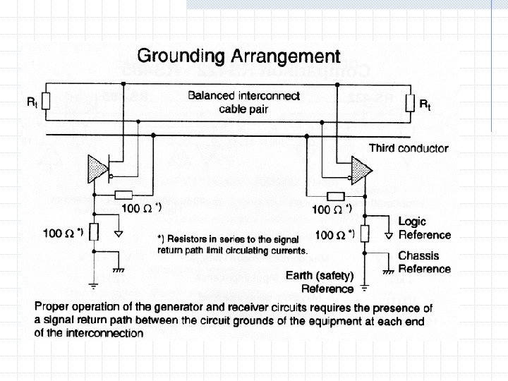
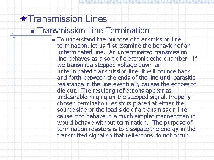
Transmission Lines n Transmission Line Termination n To understand the purpose of transmission line termination, let us first examine the behavior of an unterminated line. An unterminated transmission line behaves as a sort of electronic echo chamber. If we transmit a stepped voltage down an unterminated transmission line, it will bounce back and forth between the ends of the line until parasitic resistance in the line eventually causes the echoes to die out. The resulting reflections appear as undesirable ringing on the stepped signal. Properly chosen termination resistors placed at either the source side or the load side of a transmission line cause it to behave in a much simpler manner than it would behave without termination. The purpose of termination resistors is to dissipate the energy in the transmitted signal so that reflections do not occur.

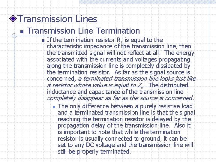
Transmission Lines n Transmission Line Termination n If the termination resistor RT is equal to the characteristic impedance of the transmission line, then the transmitted signal will not reflect at all. The energy associated with the currents and voltages propagating along the transmission line is completely dissipated by the termination resistor. As far as the signal source is concerned, a terminated transmission line looks just like a resistor whose value is equal to Zo. The distributed inductance and capacitance of the transmission line completely disappear as far as the source is concerned. n The only difference between a purely resistive load and a terminated transmission line is that the signal reaching the termination resistor is delayed by the propagation delay of the transmission line. Also it is important to note that while the termination resistor is usually connected to ground, it can be set to any DC voltage and the transmission line will still be properly terminated.

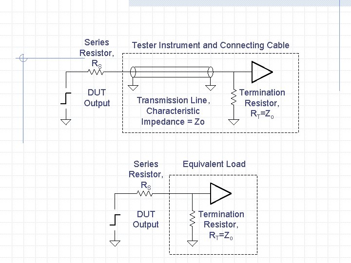
Series Resistor, RS DUT Output Tester Instrument and Connecting Cable Transmission Line, Characteristic Impedance = Zo Series Resistor, RS DUT Output Termination Resistor, RT=Zo Equivalent Load Termination Resistor, RT=Zo

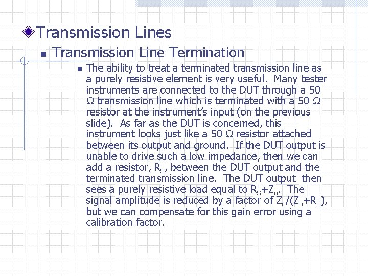
Transmission Lines n Transmission Line Termination n The ability to treat a terminated transmission line as a purely resistive element is very useful. Many tester instruments are connected to the DUT through a 50 transmission line which is terminated with a 50 resistor at the instrument’s input (on the previous slide). As far as the DUT is concerned, this instrument looks just like a 50 resistor attached between its output and ground. If the DUT output is unable to drive such a low impedance, then we can add a resistor, RS, between the DUT output and the terminated transmission line. The DUT output then sees a purely resistive load equal to RS+Zo. The signal amplitude is reduced by a factor of Zo/(Zo+RS), but we can compensate for this gain error using a calibration factor.

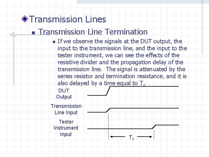
Transmission Lines n Transmission Line Termination n If we observe the signals at the DUT output, the input to the transmission line, and the input to the tester instrument, we can see the effects of the resistive divider and the propagation delay of the transmission line. The signal is attenuated by the series resistor and termination resistance, and it is also delayed by a time equal to Td. DUT Output Transmission Line Input Tester Instrument Input Td

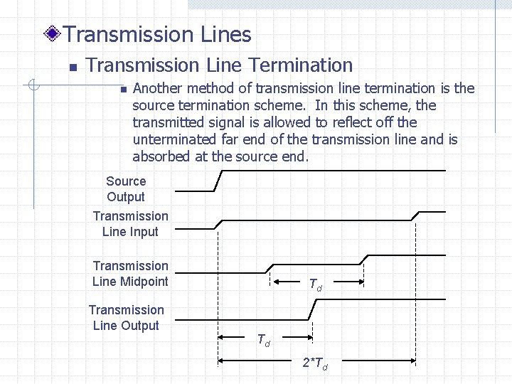
Transmission Lines n Transmission Line Termination n Another method of transmission line termination is the source termination scheme. In this scheme, the transmitted signal is allowed to reflect off the unterminated far end of the transmission line and is absorbed at the source end. Source Output Transmission Line Input Transmission Line Midpoint Transmission Line Output Td Td 2*Td

Transmission Lines n Transmission Line Termination n One of the common mistakes made by novice test engineers is to observe the output of a digital channel at the point where the DIB connects to the test head. Such an observation point represents an intermediate point along the cascaded transmission line. As a result, a rising edge will appear as a pair of transitions rather than a single transition. The novice test engineer often thinks the tester driver is defective, when in fact it is working just fine. The only way to see the correct signal is to observe it at the DUT’s input.

Transmission Lines n Transmission Line Termination n Notice that we can measure the propagation delay of a transmission line by measuring the time between the first and second step transitions at the source end of a sourceterminated transmission line. This time is equal to 2*T d. We can divide the measured time by two to calculate the transmission line’s propagation delay. This is how modern testers measure the propagation delays from the digital channel card drivers to the DUT’s digital inputs. The tester can automatically compensate for the electrical delay in each transmission line, thereby removing timing skew from the digital signals. This deskewing process is known as time domain reflectometry, or TDR.

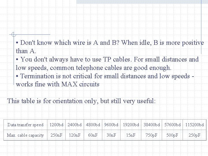
• Don't know which wire is A and B? When idle, B is more positive than A. • You don't always have to use TP cables. For small distances and low speeds, common telephone cables are good enough. • Termination is not critical for small distances and low speeds - works fine with MAX circuits This table is for orientation only, but still very useful: Data transfer speed 1200 bd 2400 bd 4800 bd 9600 bd 19200 bd Max. cable capacity 250 n. F 120 n. F 60 n. F 30 n. F 15 n. F 38400 bd 57600 bd 115200 bd 750 p. F 500 p. F 250 p. F

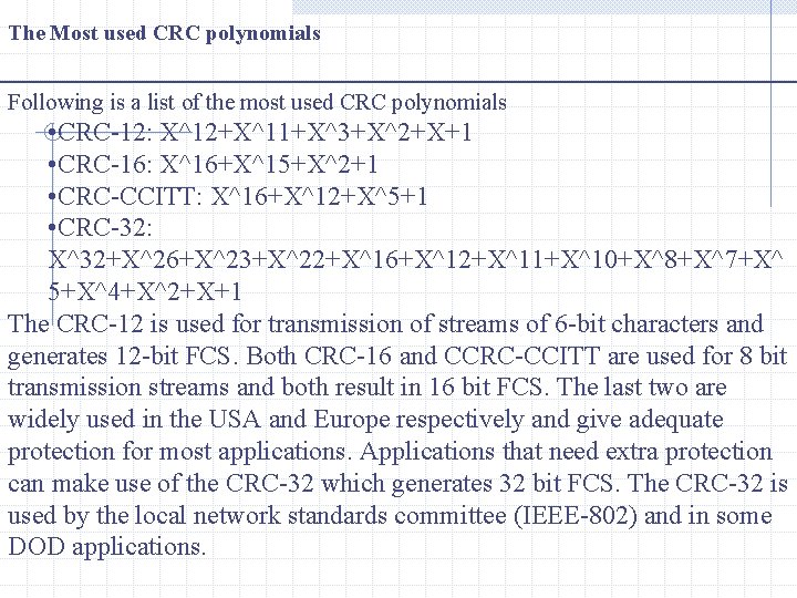
The Most used CRC polynomials Following is a list of the most used CRC polynomials • CRC-12: X^12+X^11+X^3+X^2+X+1 • CRC-16: X^16+X^15+X^2+1 • CRC-CCITT: X^16+X^12+X^5+1 • CRC-32: X^32+X^26+X^23+X^22+X^16+X^12+X^11+X^10+X^8+X^7+X^ 5+X^4+X^2+X+1 The CRC-12 is used for transmission of streams of 6 -bit characters and generates 12 -bit FCS. Both CRC-16 and CCRC-CCITT are used for 8 bit transmission streams and both result in 16 bit FCS. The last two are widely used in the USA and Europe respectively and give adequate protection for most applications. Applications that need extra protection can make use of the CRC-32 which generates 32 bit FCS. The CRC-32 is used by the local network standards committee (IEEE-802) and in some DOD applications.

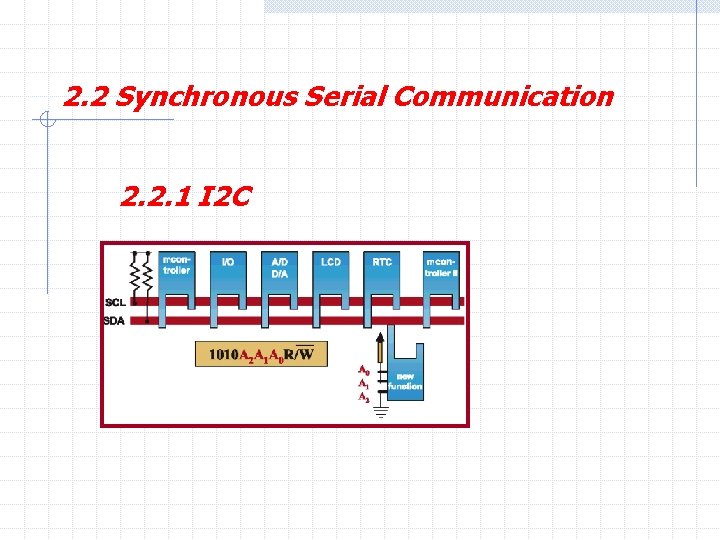
2. 2 Synchronous Serial Communication 2. 2. 1 I 2 C

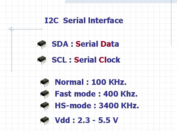
I 2 C Serial lnterface SDA : Serial Data SCL : Serial Clock Normal : 100 KHz. Fast mode : 400 Khz. HS-mode : 3400 KHz. Vdd : 2. 3 - 5. 5 V

The I C BUS 2 (Inter - Integrated Circuit) · A 2 wire serial data and control bus · Implemented with one serial data (SDA) and one clock (SCL) line. · Unique start and stop conditions. · Slave selection protocol uses a 7 -Bit slave address. · Bi-directional data transfer. · Acknowledgement after each byte transferred. · No limit on the number of bytes transferred. · Real multimaster capability.

I 2 C Bus Features · Clock synchronization. · Arbitration procedure. · Transmission speed up to 400 Khz · Maximum bus length of 4 meters. · Maximum drive capacity of 400 p. F. · Allows series resistor for IC protection. · Compatible with most IC technologies (TTL, CMOS, Etc. ).

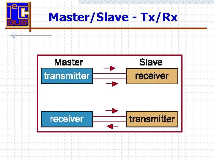
I 2 C Definitions MASTER: · Initiates a transfer by generating start and stop conditions. · Generates the clock. · Transmits the slave address. · Determines data transfer direction. SLAVE: · Responds only when addressed. · Timing is controlled by the clock line.

Master/Slave - Tx/Rx

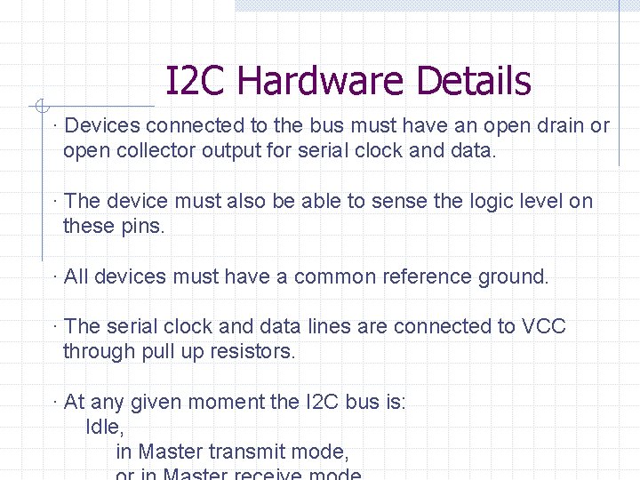
I 2 C Hardware Details · Devices connected to the bus must have an open drain or open collector output for serial clock and data. · The device must also be able to sense the logic level on these pins. · All devices must have a common reference ground. · The serial clock and data lines are connected to VCC through pull up resistors. · At any given moment the I 2 C bus is: Idle, in Master transmit mode,

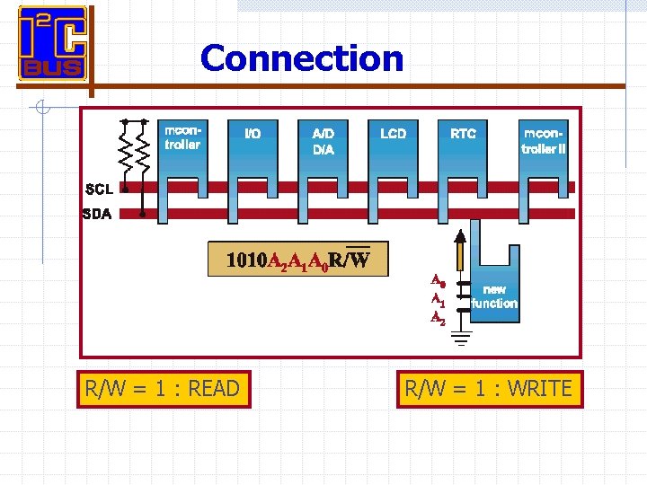
Connection R/W = 1 : READ R/W = 1 : WRITE

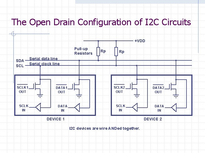
The Open Drain Configuration of I 2 C Circuits +VDD Pull-up Resistors SDA SCL Rp Rp Serial data line Serial clock line SCLK 1 OUT DATA 1 OUT SCLK 2 OUT DATA 2 OUT SCLK IN DATA IN DEVICE 1 DEVICE 2 I 2 C devices are wire ANDed together.

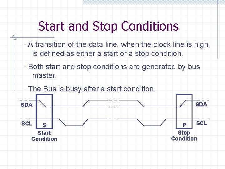
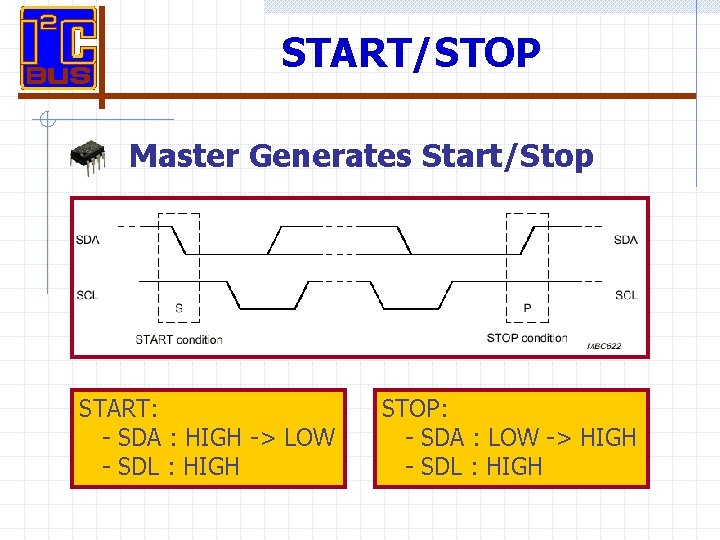
Start and Stop Conditions · A transition of the data line, when the clock line is high, is defined as either a start or a stop condition. · Both start and stop conditions are generated by bus master. · The Bus is busy after a start condition. SDA SCL P Stop Condition S Start Condition

START/STOP Master Generates Start/Stop START: - SDA : HIGH -> LOW - SDL : HIGH STOP: - SDA : LOW -> HIGH - SDL : HIGH

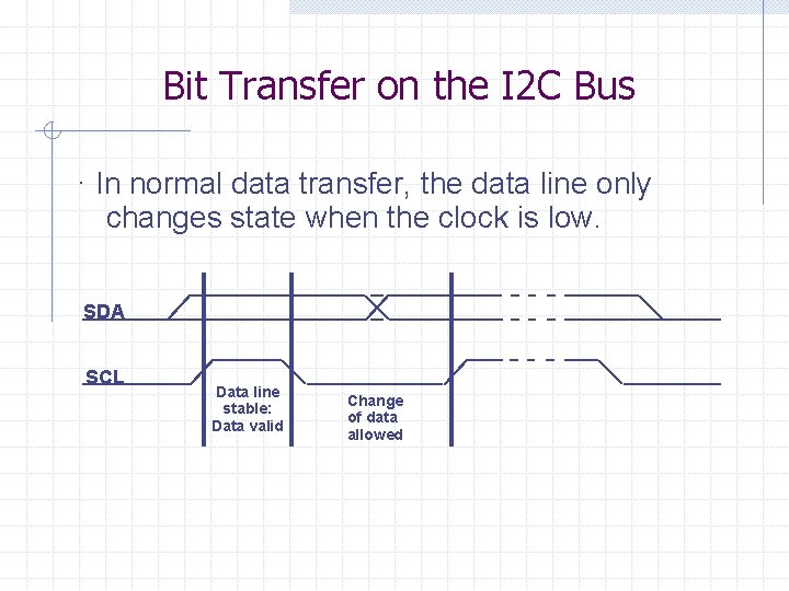
Bit Transfer on the I 2 C Bus · In normal data transfer, the data line only changes state when the clock is low. SDA SCL Data line stable: Data valid Change of data allowed

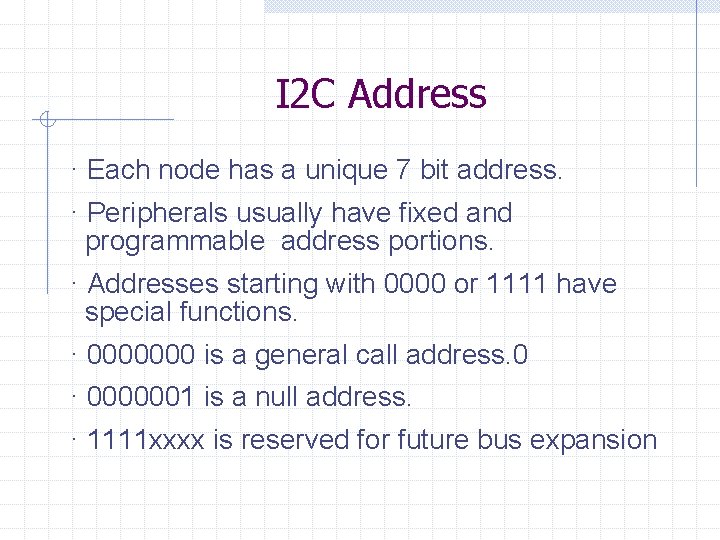
I 2 C Address · Each node has a unique 7 bit address. · Peripherals usually have fixed and programmable address portions. · Addresses starting with 0000 or 1111 have special functions. · 0000000 is a general call address. 0 · 0000001 is a null address. · 1111 xxxx is reserved for future bus expansion

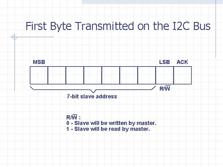
First Byte Transmitted on the I 2 C Bus MSB LSB R/W 7 -bit slave address R/W : 0 - Slave will be written by master. 1 - Slave will be read by master. ACK

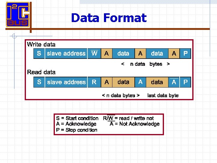
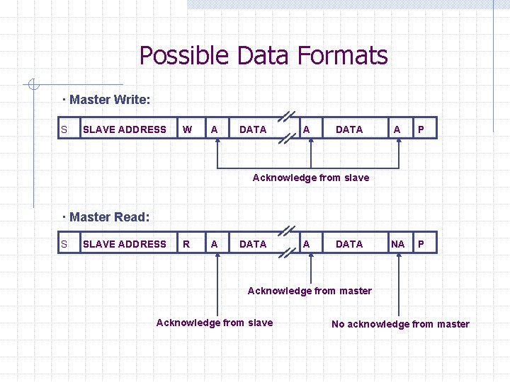
Data Format

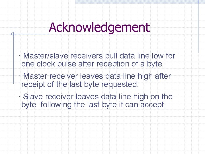
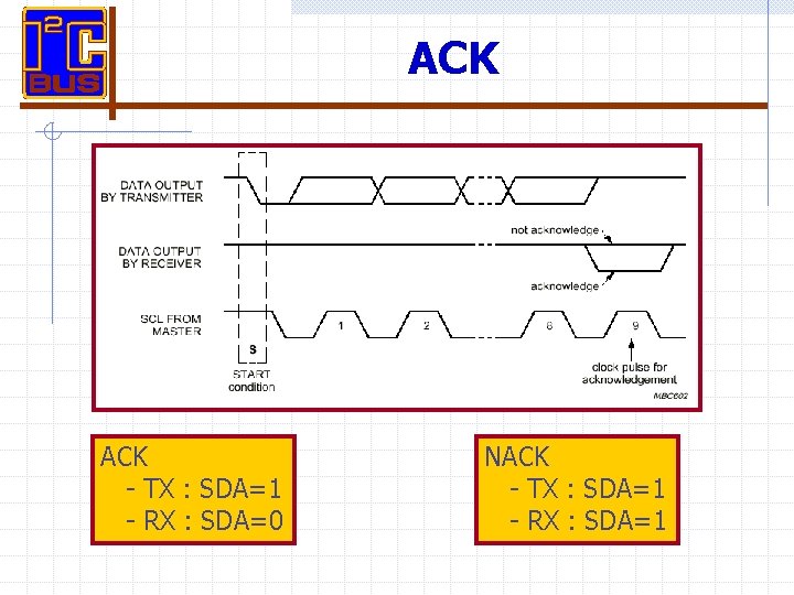
Acknowledgement · Master/slave receivers pull data line low for one clock pulse after reception of a byte. · Master receiver leaves data line high after receipt of the last byte requested. · Slave receiver leaves data line high on the byte following the last byte it can accept.

ACK - TX : SDA=1 - RX : SDA=0 NACK - TX : SDA=1 - RX : SDA=1

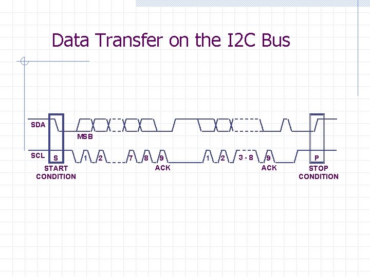
Data Transfer on the I 2 C Bus SDA MSB SCL S START CONDITION 1 2 7 8 9 ACK 1 2 3 -8 9 ACK P STOP CONDITION

Possible Data Formats · Master Write: S SLAVE ADDRESS W A DATA A P NA P Acknowledge from slave · Master Read: S SLAVE ADDRESS R A DATA Acknowledge from master Acknowledge from slave No acknowledge from master

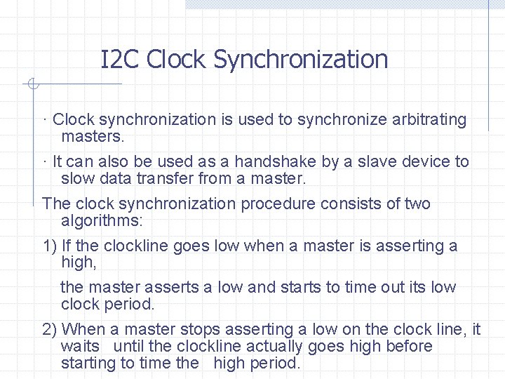
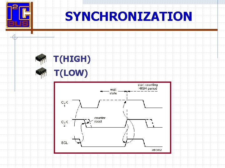
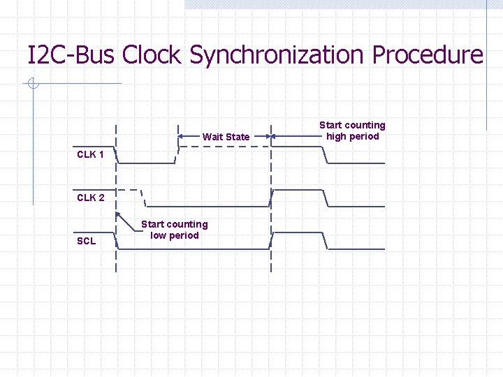
I 2 C Clock Synchronization · Clock synchronization is used to synchronize arbitrating masters. · It can also be used as a handshake by a slave device to slow data transfer from a master. The clock synchronization procedure consists of two algorithms: 1) If the clockline goes low when a master is asserting a high, the master asserts a low and starts to time out its low clock period. 2) When a master stops asserting a low on the clock line, it waits until the clockline actually goes high before starting to time the high period.

SYNCHRONIZATION T(HIGH) T(LOW)

I 2 C-Bus Clock Synchronization Procedure Wait State CLK 1 CLK 2 SCL Start counting low period Start counting high period

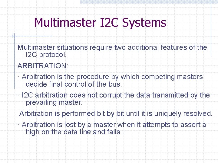
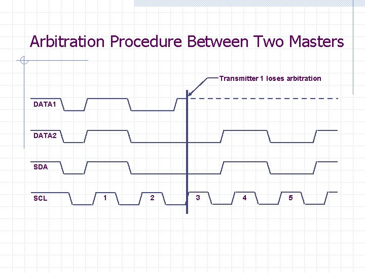
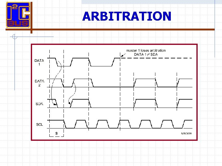
Multimaster I 2 C Systems Multimaster situations require two additional features of the I 2 C protocol. ARBITRATION: · Arbitration is the procedure by which competing masters decide final control of the bus. · I 2 C arbitration does not corrupt the data transmitted by the prevailing master. Arbitration is performed bit by bit until it is uniquely resolved. · Arbitration is lost by a master when it attempts to assert a high on the data line and fails. .

Arbitration Procedure Between Two Masters Transmitter 1 loses arbitration DATA 1 DATA 2 SDA SCL 1 2 3 4 5

ARBITRATION

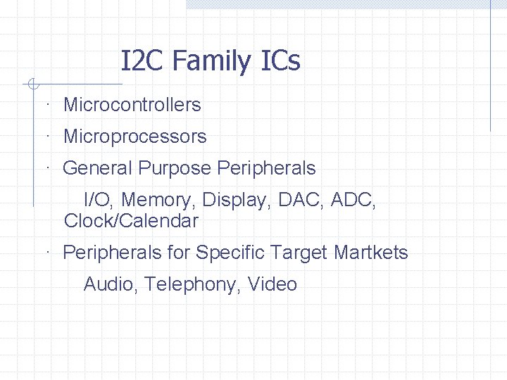
I 2 C Family ICs · Microcontrollers · Microprocessors · General Purpose Peripherals I/O, Memory, Display, DAC, ADC, Clock/Calendar · Peripherals for Specific Target Martkets Audio, Telephony, Video

ACCESS. bus. 1 DEC has invented an interconnect method for connecting a PC or Workstation to low speed I/O devices such as: · Keyboards · Mouses · Trackballs · Tablets · Low speed printers · Modems This interconnect method, known as ACCESS. bus, is based o the I 2 C serial protocol invented by Philips.

ACCESS. bus. 2 ACCESS. bus features: · 80 KBps Peak Bandwidth · Hot plugging and unplugging of devices (keyboard, mouse, etc. ) · Up to 14 devices · Up to 8 Meters (26. 4 feet) in length · Serial, daisy-chained 4 -pin cable (2 pins are power and ground). Only ONE device port needed on computer.

ACCESS Bus. 3 ACCESS. Bus features: · Layered 3 -layer protocol defined by DEC: · Physical layer is I 2 C. · Base Protocol over I 2 C defines the structure of I 2 C messages and defines Control and Status Messages. Also supports auto-addressing and hot plugging. · Applications Protocol defines message semantics for particular device types. · Extremely low cost implementation based on off-the-shelf Microcontrollers with I 2 C such as the Signetics 83/87 C 751 (used in new DEC workstation ).

ACCESS. Bus. 4 · Device address and type recognition is automatic. No drivers have to be loaded. · Concise protocol. Only 7 standard message types. Fully implemented in the 87 C 751 with 2 K of Program memory. · ACCESS. Bus is part of DEC's ARC and ACE platforms. · Fully open and free. No royalties. · DEC and Signetics will provide Developer's Kit with all information required to to develop applications. · DEC's TRI/ADD developer program will provide technical support, documentation and updates, technical seminars, and newsletters and assist with marketing support.

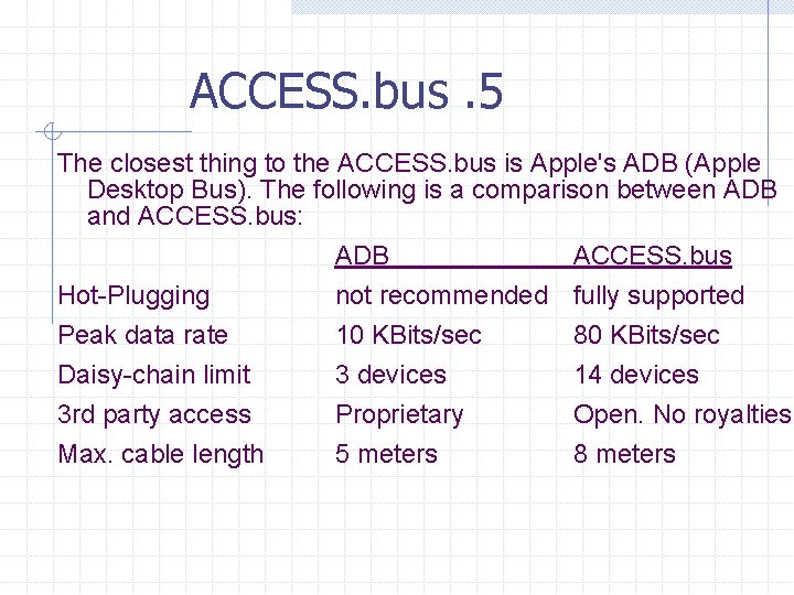
ACCESS. bus. 5 The closest thing to the ACCESS. bus is Apple's ADB (Apple Desktop Bus). The following is a comparison between ADB and ACCESS. bus: Hot-Plugging Peak data rate Daisy-chain limit 3 rd party access ADB not recommended 10 KBits/sec 3 devices Proprietary ACCESS. bus fully supported 80 KBits/sec 14 devices Open. No royalties Max. cable length 5 meters 8 meters

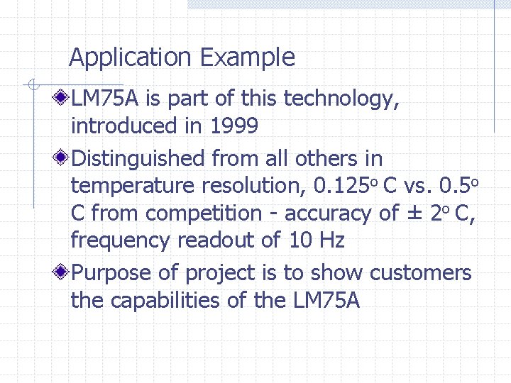
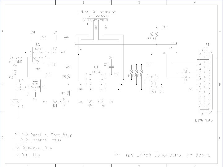
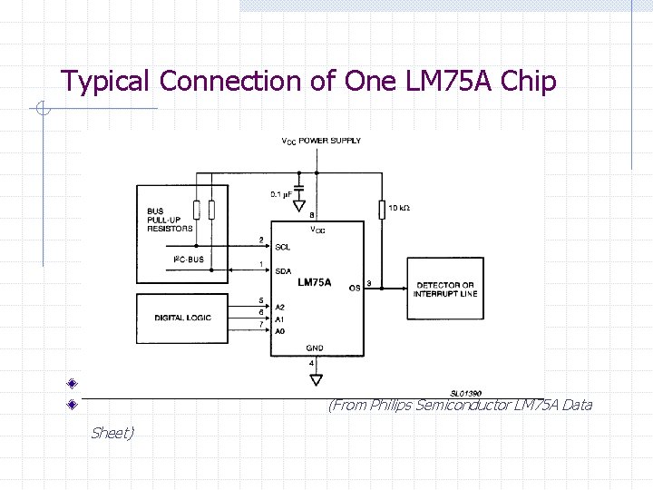
Application Example LM 75 A is part of this technology, introduced in 1999 Distinguished from all others in temperature resolution, 0. 125 o C vs. 0. 5 o C from competition - accuracy of ± 2 o C, frequency readout of 10 Hz Purpose of project is to show customers the capabilities of the LM 75 A


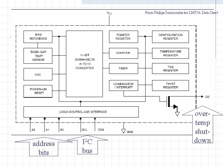
From Philips Semiconductor LM 75 A Data Sheet address bits I 2 C bus overtemp shutdown

Typical Connection of One LM 75 A Chip (From Philips Semiconductor LM 75 A Data Sheet)

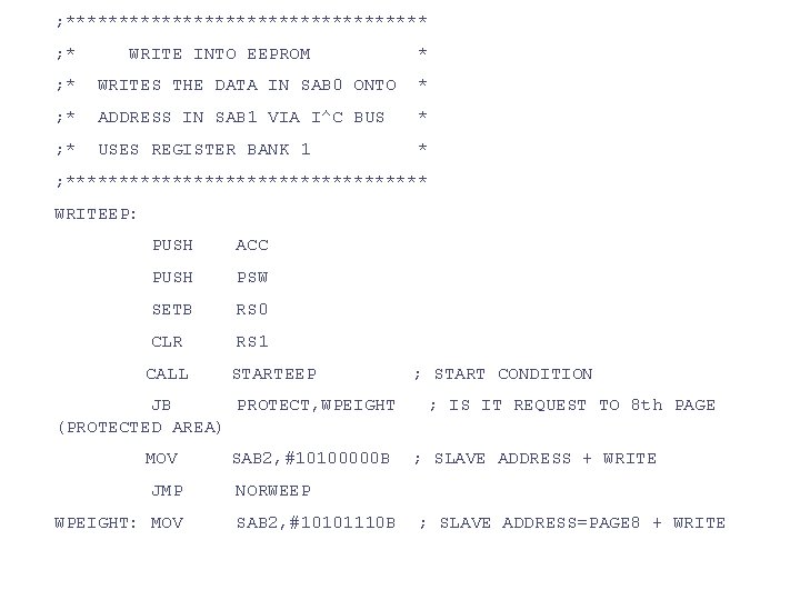
; ***************** ; * WRITE INTO EEPROM * ; * WRITES THE DATA IN SAB 0 ONTO * ; * ADDRESS IN SAB 1 VIA I^C BUS * ; * USES REGISTER BANK 1 * ; ***************** WRITEEP: PUSH ACC PUSH PSW SETB RS 0 CLR RS 1 CALL STARTEEP JB PROTECT, WPEIGHT (PROTECTED AREA) MOV JMP WPEIGHT: MOV SAB 2, #10100000 B ; START CONDITION ; IS IT REQUEST TO 8 th PAGE ; SLAVE ADDRESS + WRITE NORWEEP SAB 2, #10101110 B ; SLAVE ADDRESS=PAGE 8 + WRITE

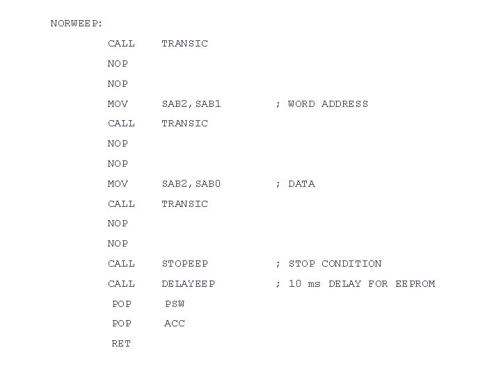
NORWEEP: CALL TRANSIC NOP MOV SAB 2, SAB 1 CALL TRANSIC ; WORD ADDRESS NOP MOV SAB 2, SAB 0 CALL TRANSIC ; DATA NOP CALL STOPEEP ; STOP CONDITION CALL DELAYEEP ; 10 ms DELAY FOR EEPROM POP PSW POP ACC RET

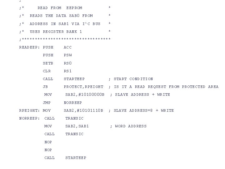
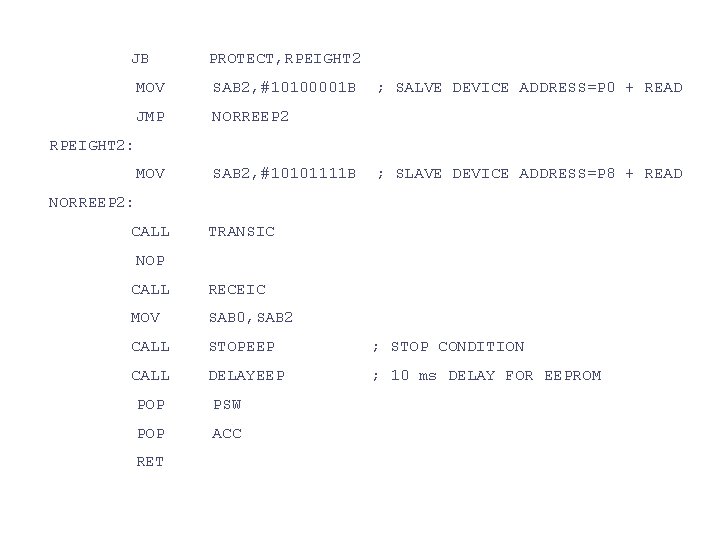
; ***************** ; * READ FROM EEPROM * ; * READS THE DATA SAB 0 FROM * ; * ADDRESS IN SAB 1 VIA I^C BUS * ; * USES REGISTER BANK 1 * ; ***************** READEEP: PUSH ACC PUSH PSW SETB RS 0 CLR RS 1 CALL STARTEEP ; START CONDITION JB PROTECT, RPEIGHT ; IS IT A READ REQUEST FROM PROTECTED AREA MOV JMP RPEIGHT: MOV NORREEP: CALL SAB 2, #10100000 B NORREEP SAB 2, #10101110 B ; SLAVE ADDRESS=8 + WRITE TRANSIC MOV SAB 2, SAB 1 CALL TRANSIC NOP CALL ; SLAVE ADDRESS + WRITE STARTEEP ; WORD ADDRESS

JB PROTECT, RPEIGHT 2 MOV SAB 2, #10100001 B JMP NORREEP 2 ; SALVE DEVICE ADDRESS=P 0 + READ RPEIGHT 2: MOV SAB 2, #10101111 B ; SLAVE DEVICE ADDRESS=P 8 + READ NORREEP 2: CALL TRANSIC NOP CALL RECEIC MOV SAB 0, SAB 2 CALL STOPEEP ; STOP CONDITION CALL DELAYEEP ; 10 ms DELAY FOR EEPROM POP PSW POP ACC RET

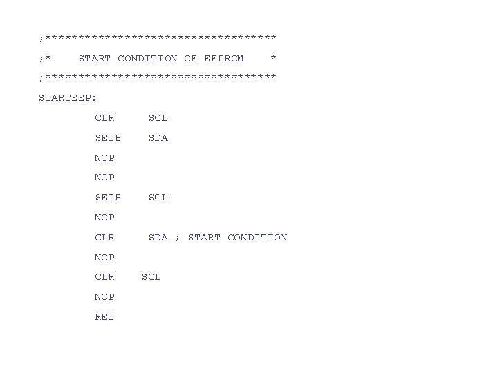
; ****************** ; * START CONDITION OF EEPROM * ; ****************** STARTEEP: CLR SCL SETB SDA NOP SETB SCL NOP CLR SDA ; START CONDITION NOP CLR NOP RET SCL

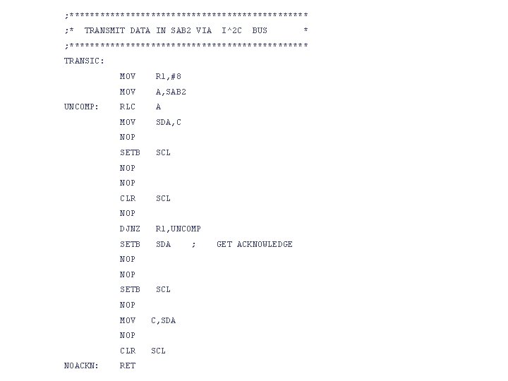
; ************************ ; * TRANSMIT DATA IN SAB 2 VIA I^2 C BUS * ; ************************ TRANSIC: UNCOMP: MOV R 1, #8 MOV A, SAB 2 RLC A MOV SDA, C NOP SETB SCL NOP CLR SCL NOP DJNZ R 1, UNCOMP SETB SDA NOP SETB SCL NOP MOV C, SDA NOP CLR NOACKN: RET SCL ; GET ACKNOWLEDGE

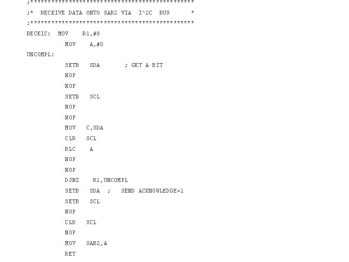
; ************************ ; * RECEIVE DATA ONTO SAB 2 VIA I^2 C BUS * ; ************************ RECEIC: MOV R 1, #8 MOV A, #0 SETB SDA UNCOMPL: ; GET A BIT NOP SETB SCL NOP MOV C, SDA CLR SCL RLC A NOP DJNZ R 1, UNCOMPL SETB SDA SETB SCL NOP ; CLR SCL NOP MOV RET SAB 2, A SEND ACKNOWLEDGE=1

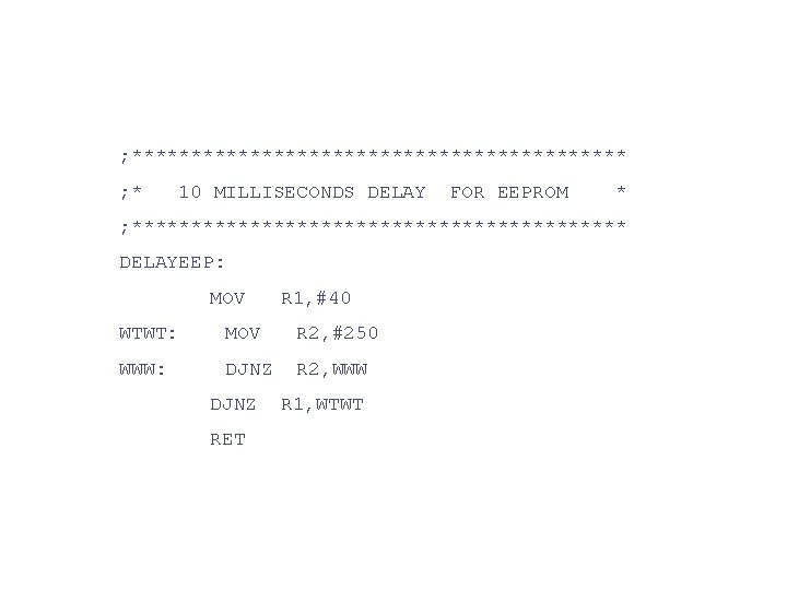
; ********************* ; * 10 MILLISECONDS DELAY FOR EEPROM * ; ********************* DELAYEEP: MOV R 1, #40 WTWT: MOV R 2, #250 WWW: DJNZ R 2, WWW DJNZ RET R 1, WTWT