16 th Workshop on Advanced Silicon Radiation Detectors
- Slides: 26

16 th Workshop on Advanced Silicon Radiation Detectors. Trento, 16 -18 february 2021 Epitaxial growth and characterization of 4 H-Si. C for detection applications Alessandro Meli La Via Francesco (CNR-imm) Muoio Annamaria (CNR-imm) Tudisco Salvatore (INFN-LNS) Trotta Antonio (ENI S. p. A. ) Parisi Miriam (ENI S. p. A. ) Meda Laura (ENI S. p. A. )

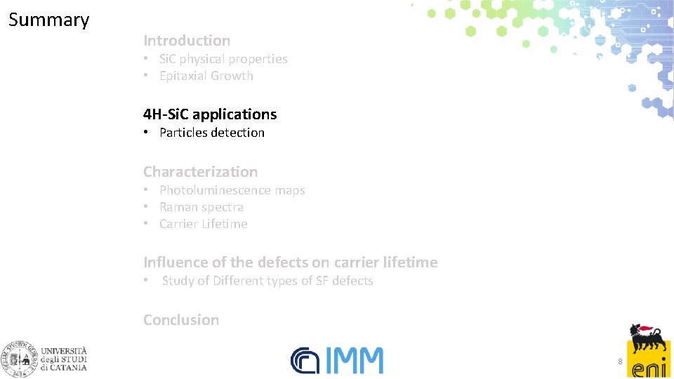
Summary Introduction • Si. C physical properties • Epitaxial Growth 4 H-Si. C applications • Particles detection Characterization • Photoluminescence maps • Raman spectra • Carrier Lifetime Influence of the defects on carrier lifetime • Study of Different types of SF defects Conclusion 2

Summary Introduction • Si. C physical properties • Epitaxial Growth 4 H-Si. C applications • Particles detection Characterization • Photoluminescence maps • Raman spectra • Carrier Lifetime Influence of the defects on carrier lifetime • Study of Different types of SF defects Conclusion 3

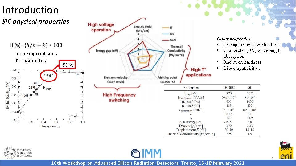
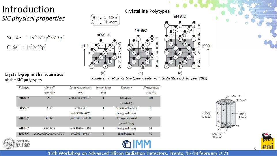
Introduction Si. C physical properties h= hexagonal sites K= cubic sites 50 % Other properties • Transparency to visible light • Ultraviolet (UV) wavelength absorption • Radiation hardness • Biocompatibility… 16 th Workshop on Advanced Silicon Radiation Detectors. Trento, 16 -18 february 2021 4

Introduction Si. C physical properties Crystallographic characteristics of the Si. C polytypes Cryistalline Polytypes Kimoto et al. , Silicon Carbide Epitaxy, edited by F. La Via (Research Signpost, 2012) 16 th Workshop on Advanced Silicon Radiation Detectors. Trento, 16 -18 february 2021 5

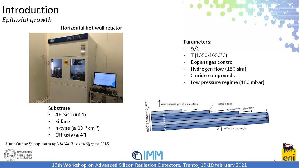
Introduction Epitaxial growth Horizontal hot-wall reactor Parameters: - Si/C - T (1550 -1650°C) - Dopant gas control - Hydrogen flow (150 slm) - Cloride compounds - Low pressure regime (100 mbar) Substrate: • 4 H-Si. C (0001) • Si face • n-type ( 1018 cm-3) • Off-axis ( 4°) Silicon Carbide Epitaxy, edited by F. La Via (Research Signpost, 2012) 16 th Workshop on Advanced Silicon Radiation Detectors. Trento, 16 -18 february 2021 6

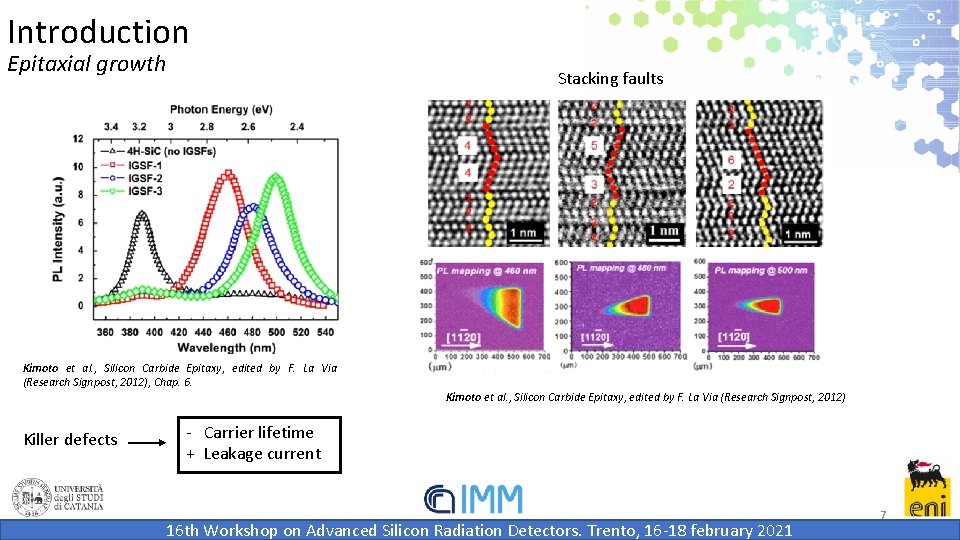
Introduction Epitaxial growth Stacking faults Kimoto et al. , Silicon Carbide Epitaxy, edited by F. La Via (Research Signpost, 2012), Chap. 6. Kimoto et al. , Silicon Carbide Epitaxy, edited by F. La Via (Research Signpost, 2012) Killer defects - Carrier lifetime + Leakage current 16 th Workshop on Advanced Silicon Radiation Detectors. Trento, 16 -18 february 2021 7

Summary Introduction • Si. C physical properties • Epitaxial Growth 4 H-Si. C applications • Particles detection Characterization • Photoluminescence maps • Raman spectra • Carrier Lifetime Influence of the defects on carrier lifetime • Study of Different types of SF defects Conclusion 8

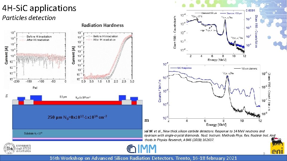
4 H-Si. C applications Particles detection Radiation Hardness S. Tudisco et al. , Eu. NPC 2018 Conference, 42 C (2019) 74. Irradiation: • 60 Me. V of H+ ions • Total dose of 2 Kgy 250 µm ND=8 x 10¹³ -1 x 1014 cm-3 • Epitaxial layer 100 µm Rebai M. et al. , New thick silicon carbide detectors: Response to 14 Me. V neutrons and comparison with single-crystal diamonds. Nucl. Instrum. Methods Phys. Res. Nuclear Inst. And Methods in Physics Research, A 946 (2019) 162637. 16 th Workshop on Advanced Silicon Radiation Detectors. Trento, 16 -18 february 2021 9

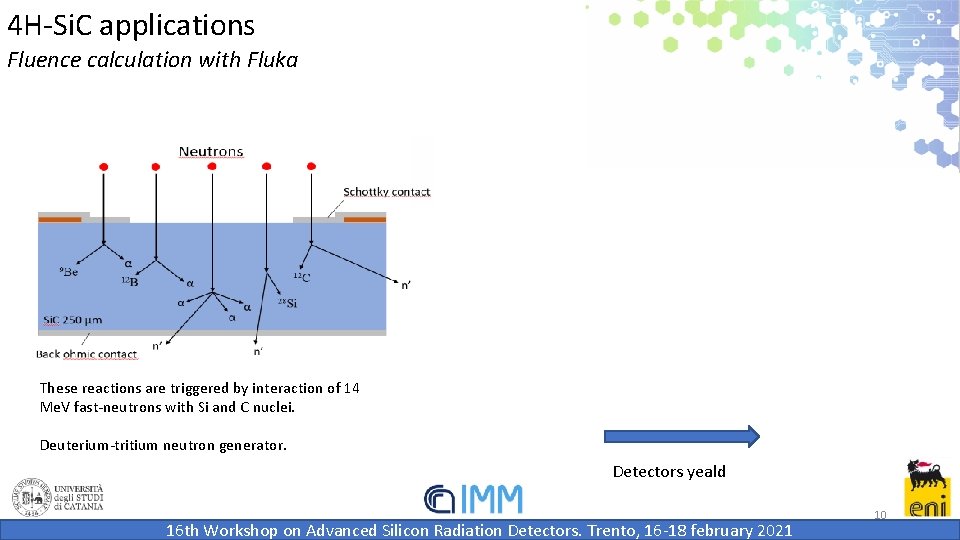
4 H-Si. C applications Fluence calculation with Fluka These reactions are triggered by interaction of 14 Me. V fast-neutrons with Si and C nuclei. Deuterium-tritium neutron generator. Detectors yeald 16 th Workshop on Advanced Silicon Radiation Detectors. Trento, 16 -18 february 2021 10

Summary Introduction • Si. C physical properties • Epitaxial Growth 4 H-Si. C applications • Particles detection Characterization • Photoluminescence maps • Raman spectra • Carrier Lifetime Influence of the defects on carrier lifetime • Study of Different types of SF defects Conclusion 11

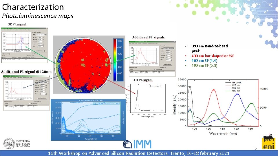
Characterization Photoluminescence maps • • 390 nm Band-to-band peak 430 nm bar shaped or SSF 460 nm SF (4, 4) 490 nm SF (5, 3) 16 th Workshop on Advanced Silicon Radiation Detectors. Trento, 16 -18 february 2021 12

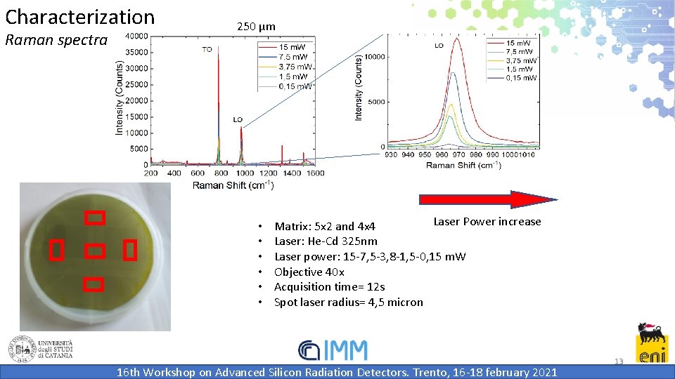
Characterization Raman spectra 250 µm • • • Laser Power increase Matrix: 5 x 2 and 4 x 4 Laser: He-Cd 325 nm Laser power: 15 -7, 5 -3, 8 -1, 5 -0, 15 m. W Objective 40 x Acquisition time= 12 s Spot laser radius= 4, 5 micron 16 th Workshop on Advanced Silicon Radiation Detectors. Trento, 16 -18 february 2021 13

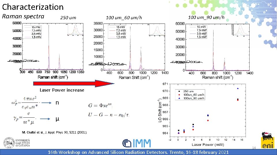
Characterization Raman spectra 250 um 100 um_60 um/h 100 um_90 um/h Laser Power increase n µ M. Chafai et al. , J. Appl. Phys. 90, 5211 (2001). 16 th Workshop on Advanced Silicon Radiation Detectors. Trento, 16 -18 february 2021 14

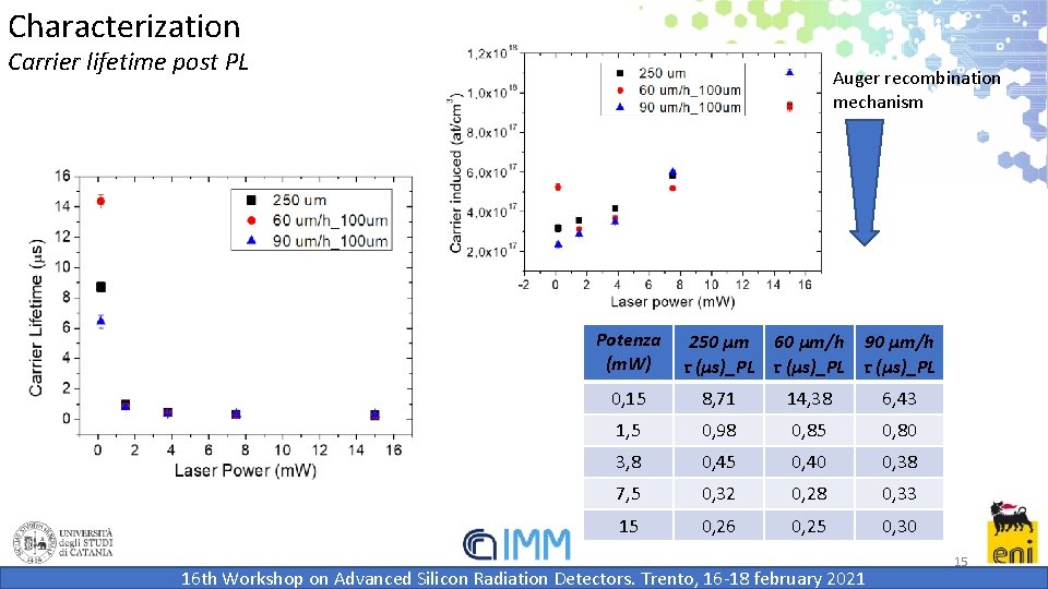
Characterization Carrier lifetime post PL Auger recombination mechanism Potenza (m. W) 250 µm 60 µm/h 90 µm/h τ (µs)_PL 0, 15 8, 71 14, 38 6, 43 1, 5 0, 98 0, 85 0, 80 3, 8 0, 45 0, 40 0, 38 7, 5 0, 32 0, 28 0, 33 15 0, 26 0, 25 0, 30 16 th Workshop on Advanced Silicon Radiation Detectors. Trento, 16 -18 february 2021 15

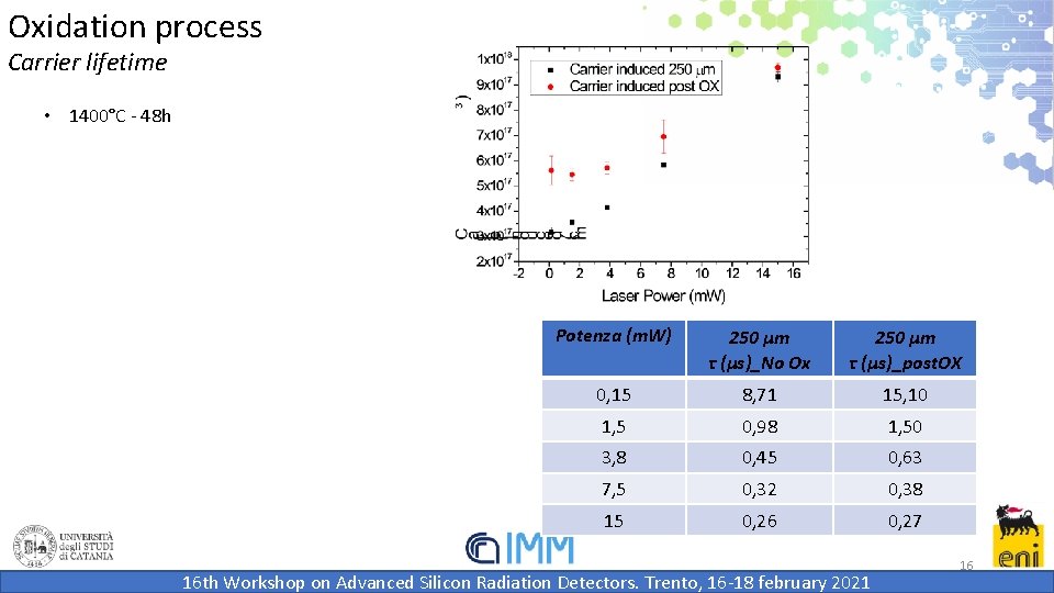
Oxidation process Carrier lifetime • 1400°C - 48 h Potenza (m. W) 250 µm τ (µs)_No Ox 250 µm τ (µs)_post. OX 0, 15 8, 71 15, 10 1, 5 0, 98 1, 50 3, 8 0, 45 0, 63 7, 5 0, 32 0, 38 15 0, 26 0, 27 16 th Workshop on Advanced Silicon Radiation Detectors. Trento, 16 -18 february 2021 16

Summary Introduction • Si. C physical properties • Epitaxial Growth 4 H-Si. C applications • Particles detection Characterization • Photoluminescence maps • Raman spectra • Carrier Lifetime Influence of the defects on carrier lifetime • Study of Different types of SF defects Conclusion 17

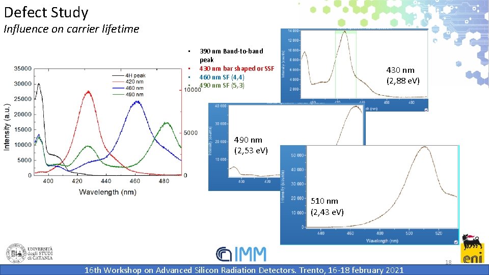
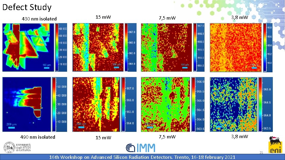
Defect Study Influence on carrier lifetime • • 390 nm Band-to-band peak 430 nm bar shaped or SSF 460 nm SF (4, 4) 490 nm SF (5, 3) 430 nm (2, 88 e. V) 490 nm (2, 53 e. V) 510 nm (2, 43 e. V) 16 th Workshop on Advanced Silicon Radiation Detectors. Trento, 16 -18 february 2021 18

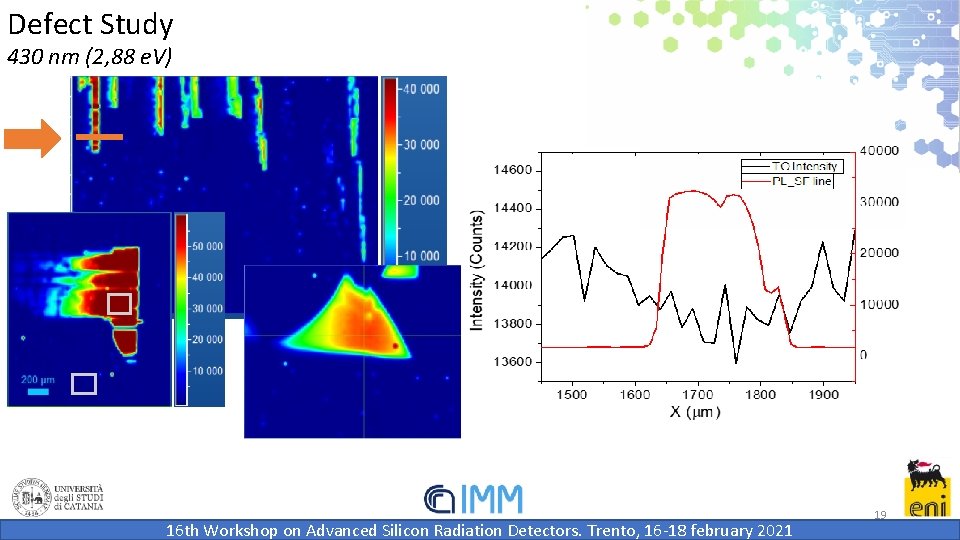
Defect Study 430 nm (2, 88 e. V) 16 th Workshop on Advanced Silicon Radiation Detectors. Trento, 16 -18 february 2021 19

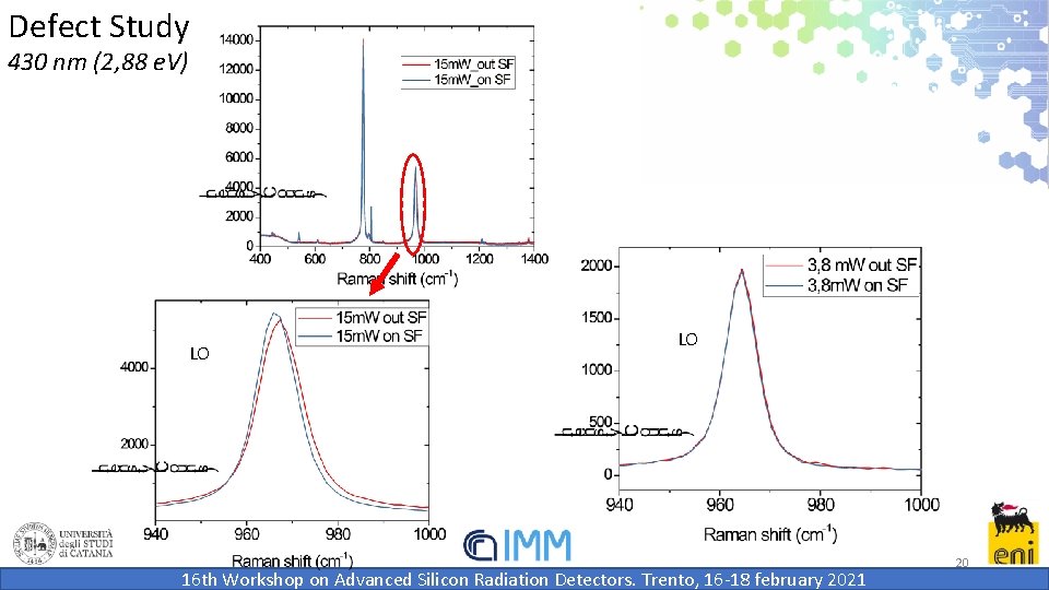
Defect Study 430 nm (2, 88 e. V) LO LO 16 th Workshop on Advanced Silicon Radiation Detectors. Trento, 16 -18 february 2021 20

Defect Study 430 nm isolated 15 m. W 7, 5 m. W 3, 8 m. W 490 nm isolated 15 m. W 7, 5 m. W 3, 8 m. W 16 th Workshop on Advanced Silicon Radiation Detectors. Trento, 16 -18 february 2021 21

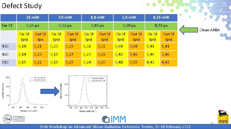
Defect Study Far SF 15 m. W 7, 5 m. W 3, 8 m. W 1, 5 m. W 0, 15 m. W 0, 26 µs 0, 32 µs 0, 45 µs 0, 98 µs 8, 71 µs On SF (µs) Out SF (µs) On SF (µs) Out SF (µs) 430 0, 18 0, 21 0, 23 0, 25 0, 31 0, 32 0, 68 5, 41 490 0, 14 0, 23 0, 17 0, 23 0, 29 0, 49 3, 46 510 0, 15 0, 22 0, 17 0, 25 0, 24 0, 30 0, 48 0, 55 4, 43 16 th Workshop on Advanced Silicon Radiation Detectors. Trento, 16 -18 february 2021 Clean AREA 22

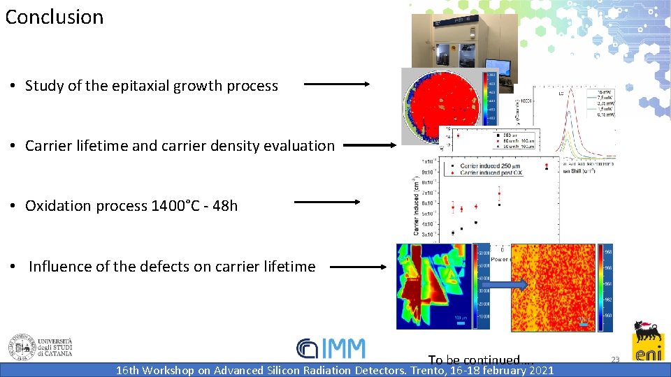
Conclusion • Study of the epitaxial growth process • Carrier lifetime and carrier density evaluation • Oxidation process 1400°C - 48 h • Influence of the defects on carrier lifetime To be continued…. 16 th Workshop on Advanced Silicon Radiation Detectors. Trento, 16 -18 february 2021 23

Acknowledgment Dott. La Via Francesco Dott. Muoio Annamaria Prof. ssa Calcagno Lucia Antonio Trotta Laura Meda Miriam Parisi 16 th Workshop on Advanced Silicon Radiation Detectors. Trento, 16 -18 february 2021 24

Thanks for your kind attention 16 th Workshop on Advanced Silicon Radiation Detectors. Trento, 16 -18 february 2021 25

16 th Workshop on Advanced Silicon Radiation Detectors. Trento, 16 -18 february 2021 26