15 74018 740 Computer Architecture Lecture 19 Main
- Slides: 30

15 -740/18 -740 Computer Architecture Lecture 19: Main Memory Prof. Onur Mutlu Carnegie Mellon University

Last Time n Multi-core issues in caching q q q OS-based cache partitioning (using page coloring) Handling shared data in caches Non-uniform cache access Caches as bandwidth filters Revisiting cache insertion policies n Dynamic insertion policy 2

Today n n n SRAM vs. DRAM Interleaving/Banking DRAM Microarchitecture q q q n n n Memory controller Memory buses Banks, ranks, channels, DIMMs Address mapping: software vs. hardware DRAM refresh Memory scheduling policies Memory power/energy management Multi-core issues q q Fairness, interference Large DRAM capacity 3

Readings n Required: q q n Mutlu and Moscibroda, “Parallelism-Aware Batch Scheduling: Enabling High-Performance and Fair Memory Controllers, ” IEEE Micro Top Picks 2009. Mutlu and Moscibroda, “Stall-Time Fair Memory Access Scheduling for Chip Multiprocessors, ” MICRO 2007. Recommended: q q q Zhang et al. , “A Permutation-based Page Interleaving Scheme to Reduce Row-buffer Conflicts and Exploit Data Locality, ” MICRO 2000. Lee et al. , “Prefetch-Aware DRAM Controllers, ” MICRO 2008. Rixner et al. , “Memory Access Scheduling, ” ISCA 2000. 4

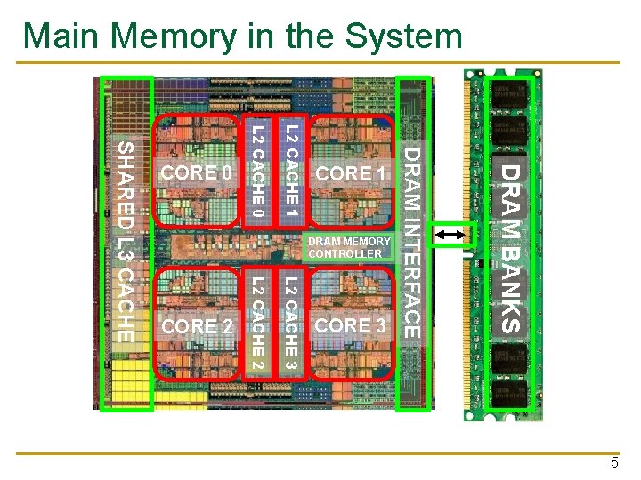
Main Memory in the System DRAM BANKS L 2 CACHE 3 L 2 CACHE 2 SHARED L 3 CACHE DRAM MEMORY CONTROLLER DRAM INTERFACE L 2 CACHE 1 L 2 CACHE 0 CORE 3 CORE 2 CORE 1 CORE 0 5

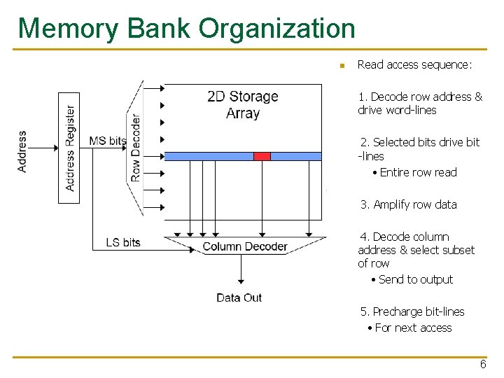
Memory Bank Organization n Read access sequence: 1. Decode row address & drive word-lines 2. Selected bits drive bit -lines • Entire row read 3. Amplify row data 4. Decode column address & select subset of row • Send to output 5. Precharge bit-lines • For next access 6

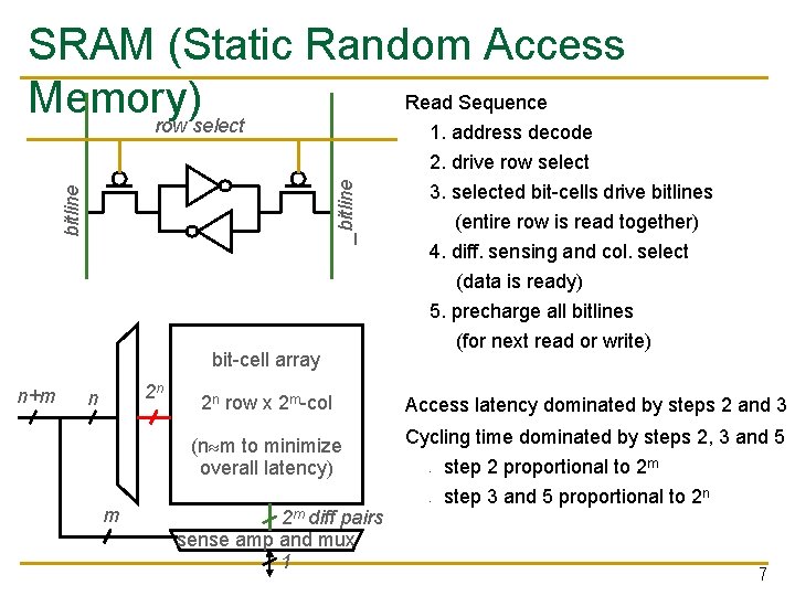
bitline _bitline SRAM (Static Random Access Read Sequence Memory) row select bit-cell array n+m 2 n n m 1. address decode 2. drive row select 3. selected bit-cells drive bitlines (entire row is read together) 4. diff. sensing and col. select (data is ready) 5. precharge all bitlines (for next read or write) 2 n row x 2 m-col Access latency dominated by steps 2 and 3 (n m to minimize overall latency) Cycling time dominated by steps 2, 3 and 5 - 2 m diff pairs sense amp and mux 1 step 2 proportional to 2 m step 3 and 5 proportional to 2 n 7

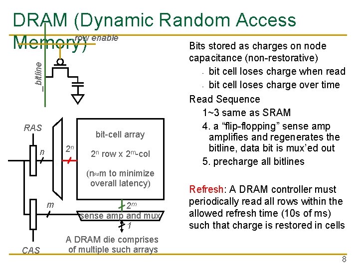
_bitline DRAM (Dynamic Random Access row enable Memory) Bits stored as charges on node RAS bit-cell array 2 n n 2 n row x 2 m-col (n m to minimize overall latency) m CAS 2 m sense amp and mux 1 capacitance (non-restorative) - bit cell loses charge when read - bit cell loses charge over time Read Sequence 1~3 same as SRAM 4. a “flip-flopping” sense amplifies and regenerates the bitline, data bit is mux’ed out 5. precharge all bitlines Refresh: A DRAM controller must periodically read all rows within the allowed refresh time (10 s of ms) such that charge is restored in cells A DRAM die comprises of multiple such arrays 8

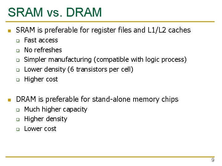
SRAM vs. DRAM n SRAM is preferable for register files and L 1/L 2 caches q q q n Fast access No refreshes Simpler manufacturing (compatible with logic process) Lower density (6 transistors per cell) Higher cost DRAM is preferable for stand-alone memory chips q q q Much higher capacity Higher density Lower cost 9

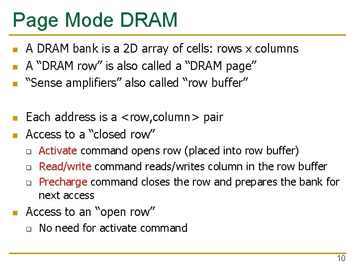
Page Mode DRAM n n n A DRAM bank is a 2 D array of cells: rows x columns A “DRAM row” is also called a “DRAM page” “Sense amplifiers” also called “row buffer” Each address is a <row, column> pair Access to a “closed row” q q q n Activate command opens row (placed into row buffer) Read/write command reads/writes column in the row buffer Precharge command closes the row and prepares the bank for next access Access to an “open row” q No need for activate command 10

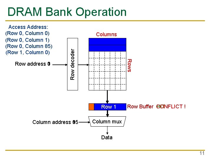
DRAM Bank Operation Rows Row address 0 1 Columns Row decoder Access Address: (Row 0, Column 0) (Row 0, Column 1) (Row 0, Column 85) (Row 1, Column 0) Row 01 Row Empty Column address 0 1 85 Row Buffer CONFLICT HIT ! Column mux Data 11

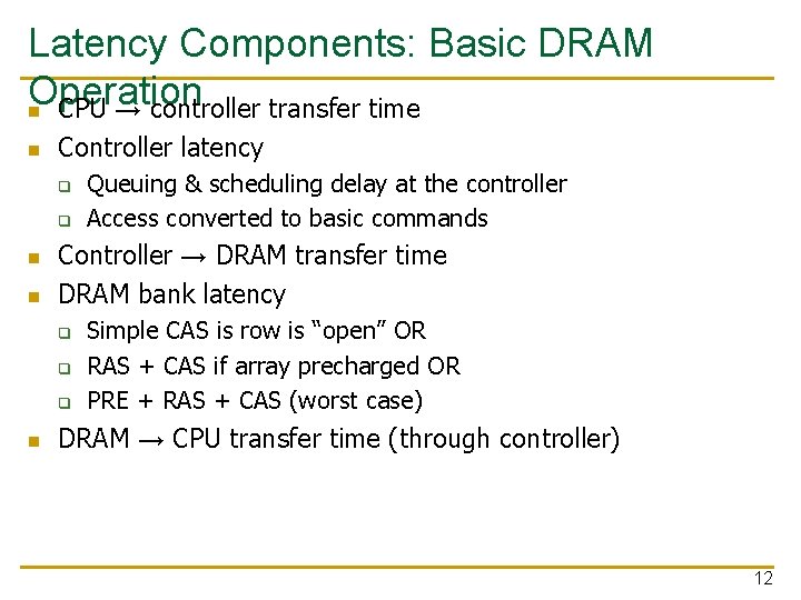
Latency Components: Basic DRAM Operation n CPU → controller transfer time n Controller latency q q n n Controller → DRAM transfer time DRAM bank latency q q q n Queuing & scheduling delay at the controller Access converted to basic commands Simple CAS is row is “open” OR RAS + CAS if array precharged OR PRE + RAS + CAS (worst case) DRAM → CPU transfer time (through controller) 12

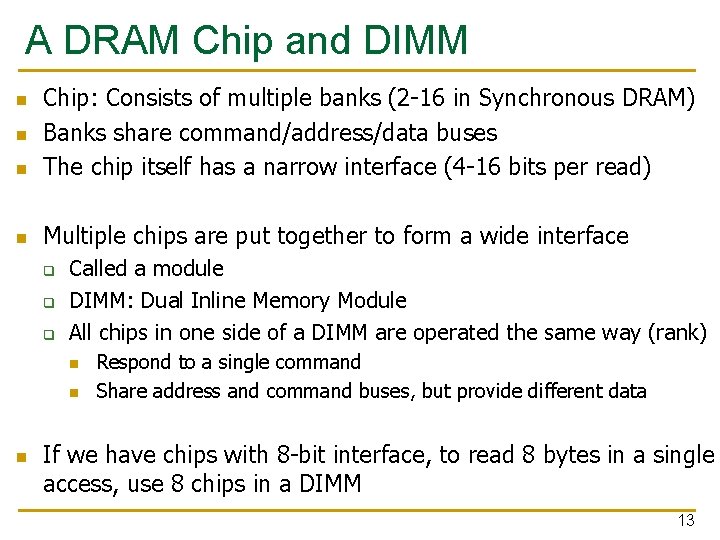
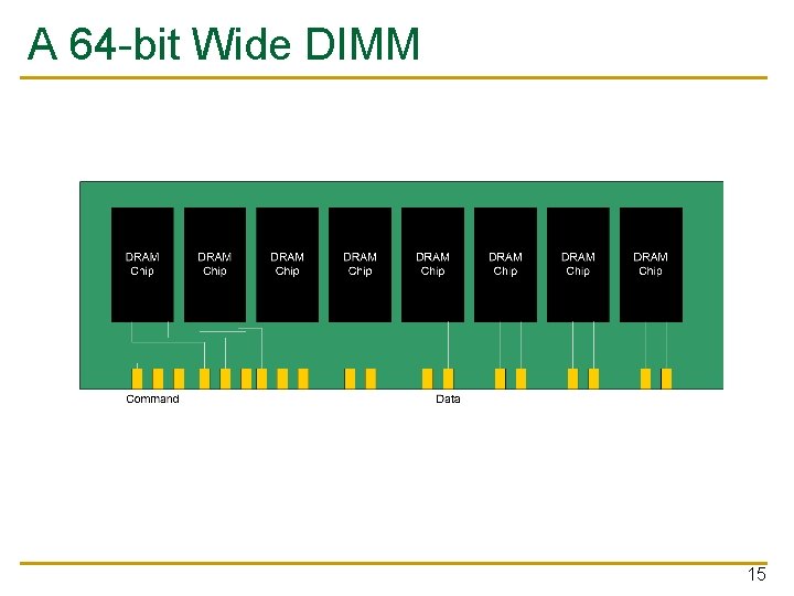
A DRAM Chip and DIMM n Chip: Consists of multiple banks (2 -16 in Synchronous DRAM) Banks share command/address/data buses The chip itself has a narrow interface (4 -16 bits per read) n Multiple chips are put together to form a wide interface n n q q q Called a module DIMM: Dual Inline Memory Module All chips in one side of a DIMM are operated the same way (rank) n n n Respond to a single command Share address and command buses, but provide different data If we have chips with 8 -bit interface, to read 8 bytes in a single access, use 8 chips in a DIMM 13

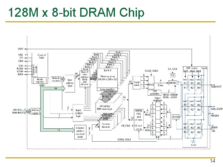
128 M x 8 -bit DRAM Chip 14

A 64 -bit Wide DIMM 15

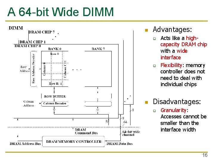
A 64 -bit Wide DIMM n Advantages: q q n Acts like a highcapacity DRAM chip with a wide interface Flexibility: memory controller does not need to deal with individual chips Disadvantages: q Granularity: Accesses cannot be smaller than the interface width 16

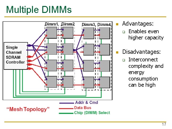
Multiple DIMMs n Advantages: q n Enables even higher capacity Disadvantages: q Interconnect complexity and energy consumption can be high 17

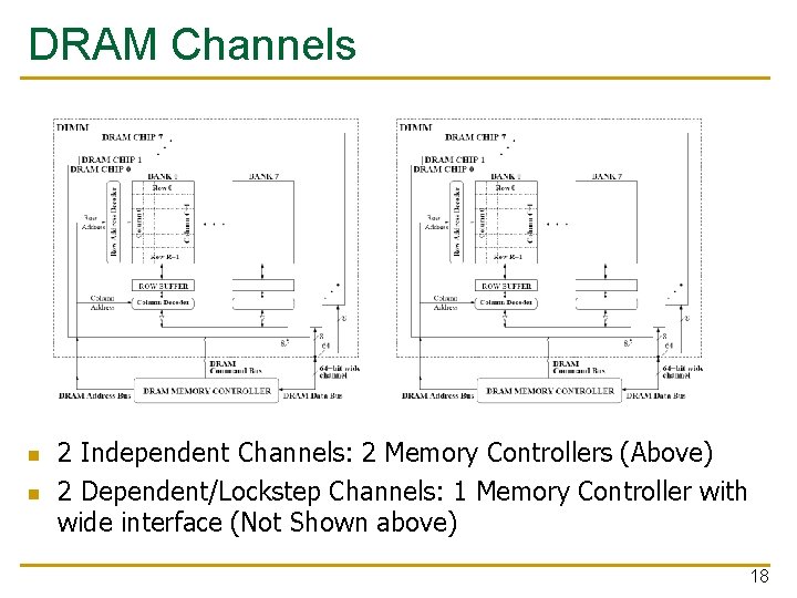
DRAM Channels n n 2 Independent Channels: 2 Memory Controllers (Above) 2 Dependent/Lockstep Channels: 1 Memory Controller with wide interface (Not Shown above) 18

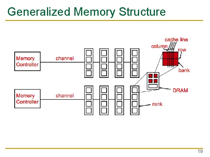
Generalized Memory Structure 19

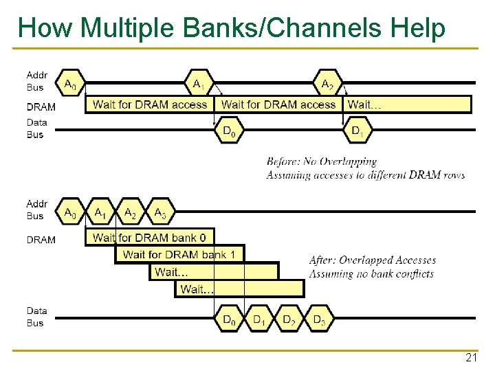
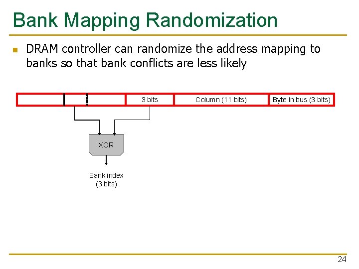
Multiple Banks (Interleaving) and n. Channels Multiple banks q q n Multiple independent channels serve the same purpose q q n But they are even better because they have separate data buses Increased bus bandwidth Enabling more concurrency requires reducing q q n Enable concurrent DRAM accesses Bits in address determine which bank an address resides in Bank conflicts Channel conflicts How to select/randomize bank/channel indices in address? q q Lower order bits have more entropy Randomizing hash functions (XOR of different address bits) 20

How Multiple Banks/Channels Help 21

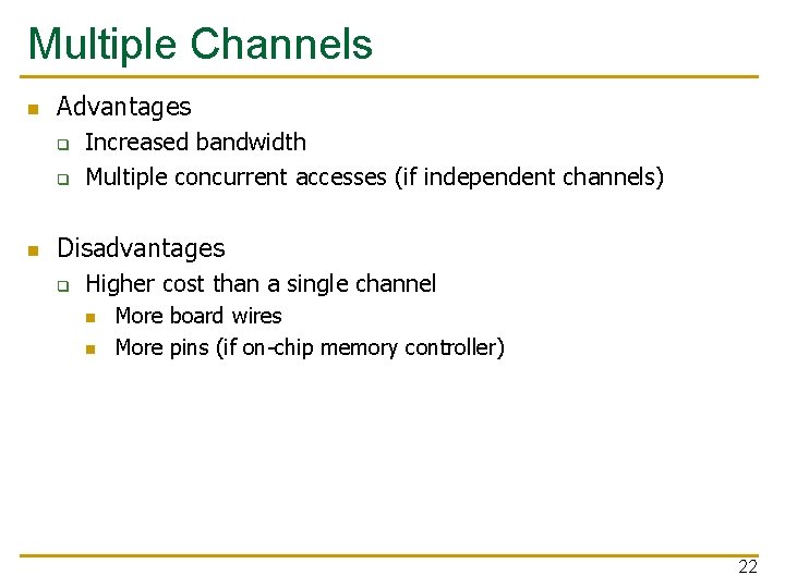
Multiple Channels n Advantages q q n Increased bandwidth Multiple concurrent accesses (if independent channels) Disadvantages q Higher cost than a single channel n n More board wires More pins (if on-chip memory controller) 22

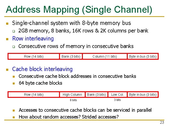
Address Mapping (Single Channel) n Single-channel system with 8 -byte memory bus q n 2 GB memory, 8 banks, 16 K rows & 2 K columns per bank Row interleaving q Consecutive rows of memory in consecutive banks Row (14 bits) n Bank (3 bits) Column (11 bits) Byte in bus (3 bits) Cache block interleaving n n Consecutive cache block addresses in consecutive banks 64 byte cache blocks Row (14 bits) High Column 8 bits n n Bank (3 bits) Low Col. Byte in bus (3 bits) 3 bits Accesses to consecutive cache blocks can be serviced in parallel How about random accesses? Strided accesses? 23

Bank Mapping Randomization n DRAM controller can randomize the address mapping to banks so that bank conflicts are less likely 3 bits Column (11 bits) Byte in bus (3 bits) XOR Bank index (3 bits) 24

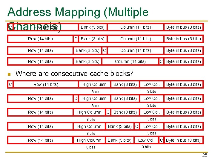
Address Mapping (Multiple Channels) C Row (14 bits) n C Bank (3 bits) Column (11 bits) Byte in bus (3 bits) Row (14 bits) Bank (3 bits) Column (11 bits) C Byte in bus (3 bits) Where are consecutive cache blocks? Row (14 bits) High Column Bank (3 bits) Low Col. 3 bits 8 bits Row (14 bits) C High Column Bank (3 bits) Low Col. High Column C Bank (3 bits) Low Col. High Column Bank (3 bits) C High Column 8 bits Low Col. Byte in bus (3 bits) 3 bits 8 bits Row (14 bits) Byte in bus (3 bits) Bank (3 bits) Low Col. C Byte in bus (3 bits) 3 bits 25

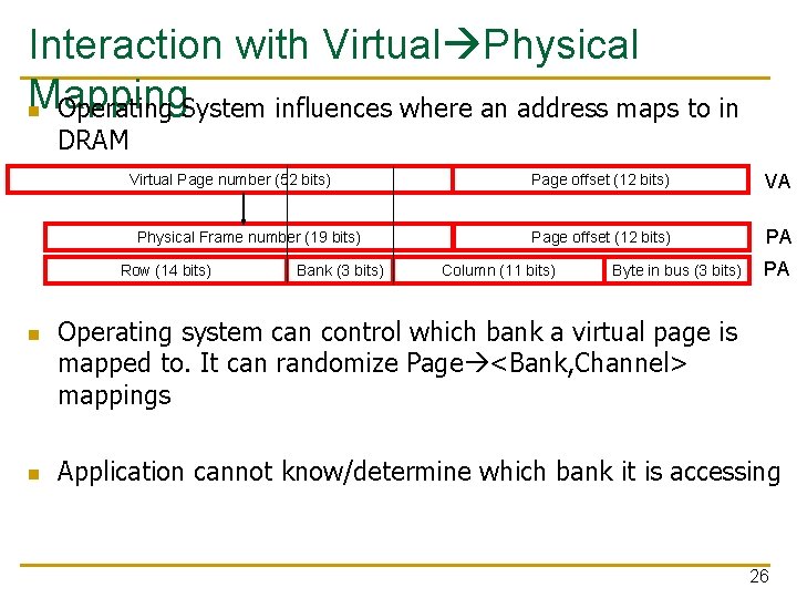
Interaction with Virtual Physical Mapping n Operating System influences where an address maps to in DRAM Virtual Page number (52 bits) Physical Frame number (19 bits) Row (14 bits) n n Bank (3 bits) Page offset (12 bits) VA Page offset (12 bits) PA Column (11 bits) Byte in bus (3 bits) PA Operating system can control which bank a virtual page is mapped to. It can randomize Page <Bank, Channel> mappings Application cannot know/determine which bank it is accessing 26

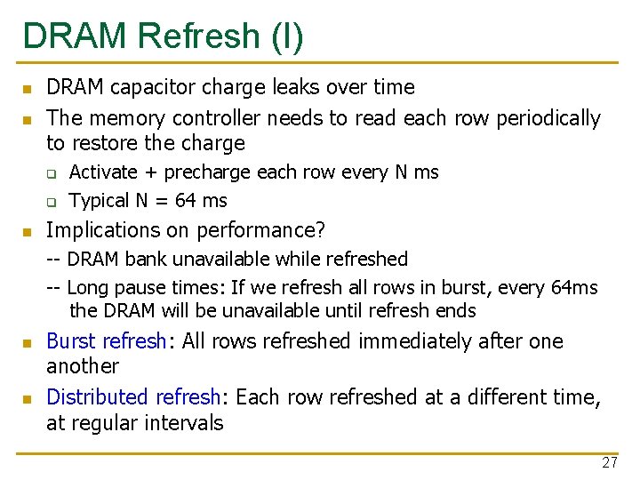
DRAM Refresh (I) n n DRAM capacitor charge leaks over time The memory controller needs to read each row periodically to restore the charge q q n Activate + precharge each row every N ms Typical N = 64 ms Implications on performance? -- DRAM bank unavailable while refreshed -- Long pause times: If we refresh all rows in burst, every 64 ms the DRAM will be unavailable until refresh ends n n Burst refresh: All rows refreshed immediately after one another Distributed refresh: Each row refreshed at a different time, at regular intervals 27

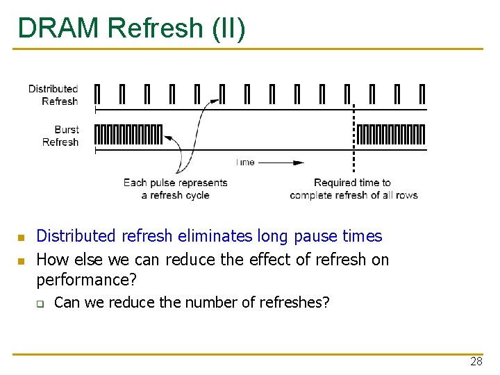
DRAM Refresh (II) n n Distributed refresh eliminates long pause times How else we can reduce the effect of refresh on performance? q Can we reduce the number of refreshes? 28

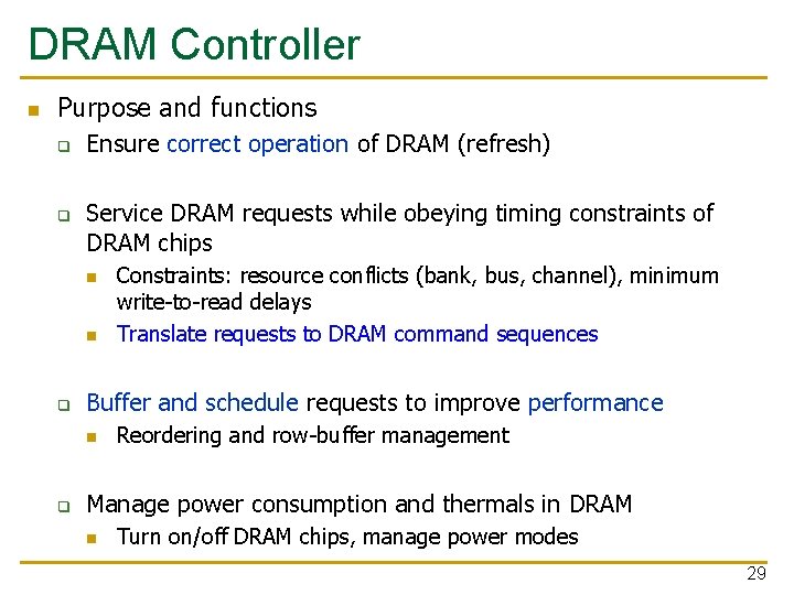
DRAM Controller n Purpose and functions q q Ensure correct operation of DRAM (refresh) Service DRAM requests while obeying timing constraints of DRAM chips n n q Buffer and schedule requests to improve performance n q Constraints: resource conflicts (bank, bus, channel), minimum write-to-read delays Translate requests to DRAM command sequences Reordering and row-buffer management Manage power consumption and thermals in DRAM n Turn on/off DRAM chips, manage power modes 29

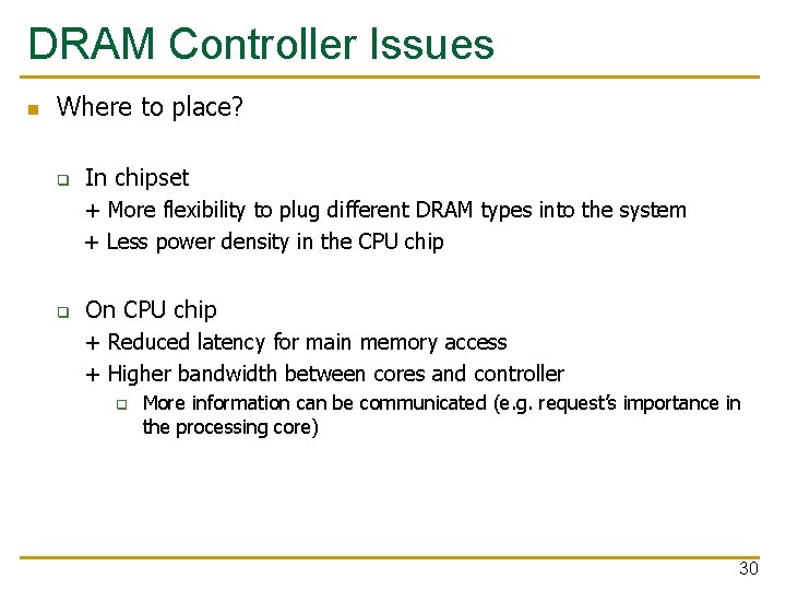
DRAM Controller Issues n Where to place? q In chipset + More flexibility to plug different DRAM types into the system + Less power density in the CPU chip q On CPU chip + Reduced latency for main memory access + Higher bandwidth between cores and controller q More information can be communicated (e. g. request’s importance in the processing core) 30