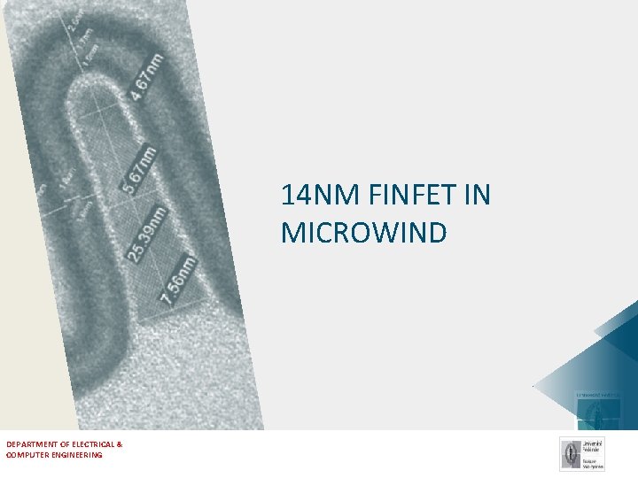
14 NM FINFET IN MICROWIND DEPARTMENT OF ELECTRICAL

- Slides: 64

14 NM FINFET IN MICROWIND DEPARTMENT OF ELECTRICAL & COMPUTER ENGINEERING

14 -NM FINFET IN MICROWIND • An application note on 14 -nm Fin. FET has been released in June 2017 • Microwind 3. 8 has been configured to simulate Fin. FET design • Technology parameters are close to 14 -nm from Intel • The rule file cmos 14 nm. RUL is available at www. microwind. org

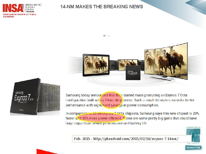
14 -NM MAKES THE BREAKING NEWS Feb. 2015 - http: //phandroid. com/2015/02/16/exynos-7 -14 nm/

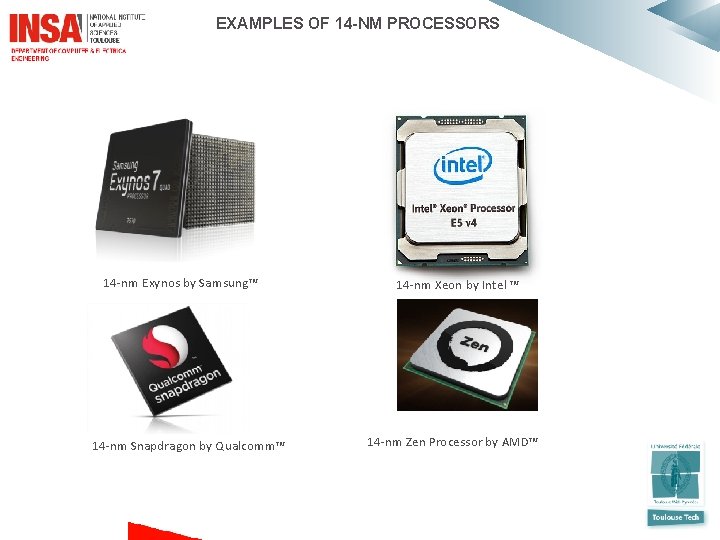
EXAMPLES OF 14 -NM PROCESSORS 14 -nm Exynos by Samsung™ 14 -nm Snapdragon by Qualcomm™ 14 -nm Xeon by Intel ™ 14 -nm Zen Processor by AMD™

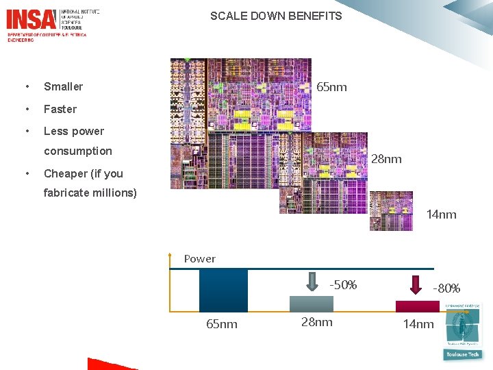
SCALE DOWN BENEFITS • Smaller • Faster • Less power 65 nm consumption • 28 nm Cheaper (if you fabricate millions) 14 nm Power -50% 65 nm 28 nm -80% 14 nm

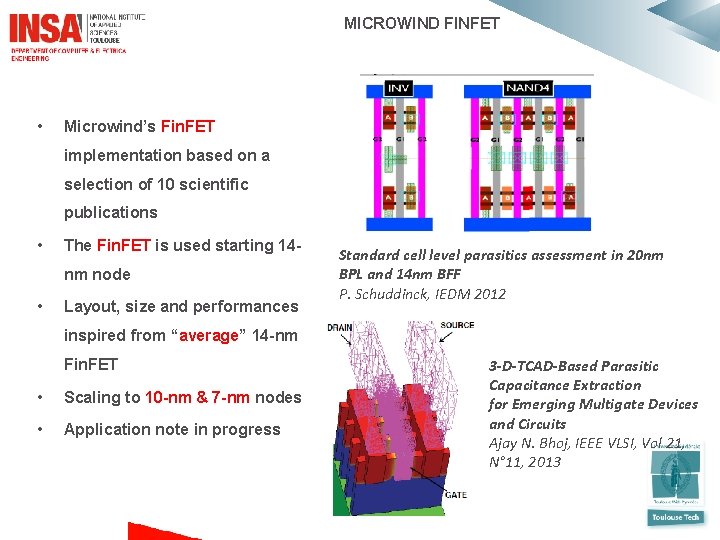
MICROWIND FINFET • Microwind’s Fin. FET implementation based on a selection of 10 scientific publications • The Fin. FET is used starting 14 nm node • Layout, size and performances Standard cell level parasitics assessment in 20 nm BPL and 14 nm BFF P. Schuddinck, IEDM 2012 inspired from “average” 14 -nm Fin. FET • Scaling to 10 -nm & 7 -nm nodes • Application note in progress 3 -D-TCAD-Based Parasitic Capacitance Extraction for Emerging Multigate Devices and Circuits Ajay N. Bhoj, IEEE VLSI, Vol 21, N° 11, 2013

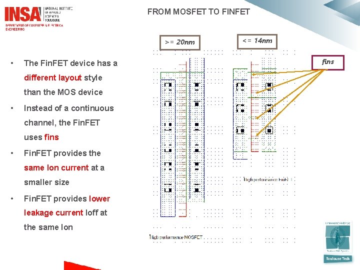
FROM MOSFET TO FINFET >= 20 nm • The Fin. FET device has a different layout style than the MOS device • Instead of a continuous channel, the Fin. FET uses fins • Fin. FET provides the same Ion current at a smaller size • Fin. FET provides lower leakage current Ioff at the same Ion <= 14 nm fins

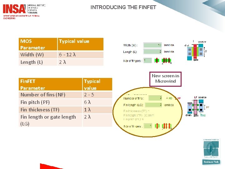
INTRODUCING THE FINFET MOS Parameter Width (W) Length (L) Typical value 6 - 12 λ Fin. FET Parameter Number of fins (NF) Fin pitch (PF) Fin thickness (TF) Fin length or gate length (LG) Typical value 2 - 5 6 λ 1 λ 2 λ New screen in Microwind

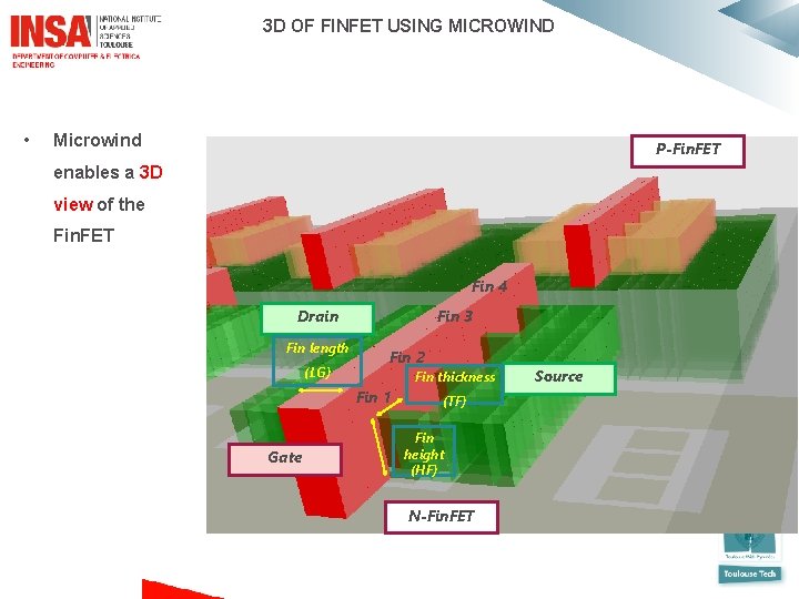
3 D OF FINFET USING MICROWIND • Microwind P-Fin. FET enables a 3 D view of the Fin. FET Fin 4 Fin 3 Drain Fin length (LG) Fin 2 Fin thickness Fin 1 Gate (TF) Fin height (HF) N-Fin. FET Source

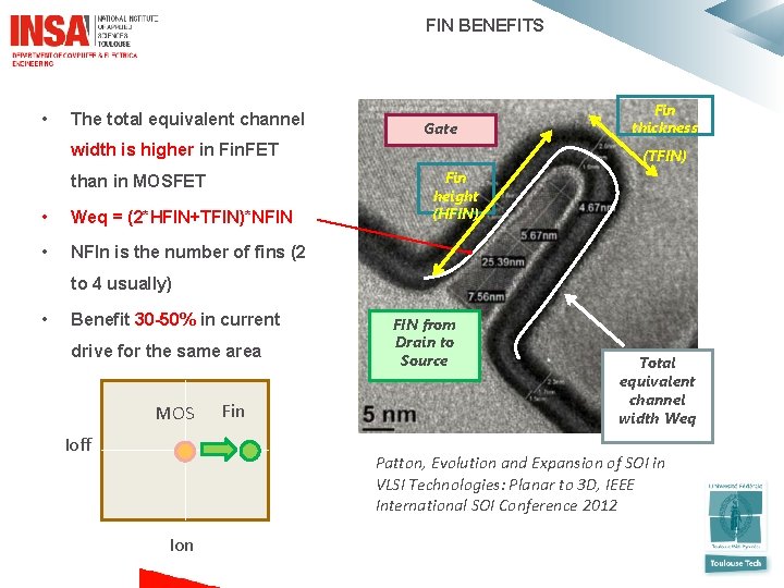
FIN BENEFITS • The total equivalent channel Gate width is higher in Fin. FET than in MOSFET • Weq = (2*HFIN+TFIN)*NFIN • NFIn is the number of fins (2 Fin thickness (TFIN) Fin height (HFIN) to 4 usually) • Benefit 30 -50% in current drive for the same area MOS Ioff Fin FIN from Drain to Source Total equivalent channel width Weq Patton, Evolution and Expansion of SOI in VLSI Technologies: Planar to 3 D, IEEE International SOI Conference 2012 Ion

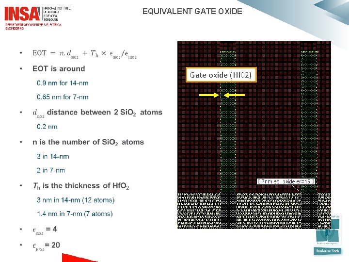
EQUIVALENT GATE OXIDE • Gate oxide (Hf 02)

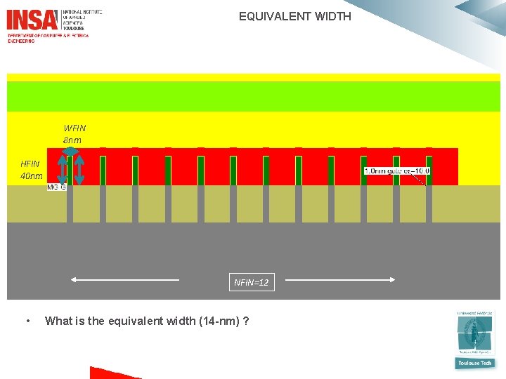
EQUIVALENT WIDTH WFIN 8 nm HFIN 40 nm NFIN=12 • What is the equivalent width (14 -nm) ?

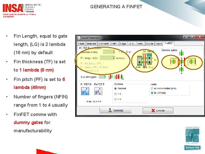
GENERATING A FINFET • Fin Length, equal to gate length, (LG) is 2 lambda (16 nm) by default • Fin thickness (TF) is set to 1 lambda (8 nm) • Fin pitch (PF) is set to 6 lambda (48 nm) • Number of fingers (NFIN) range from 1 to 4 usually • Fin. FET comme with dummy gates for manufacturability

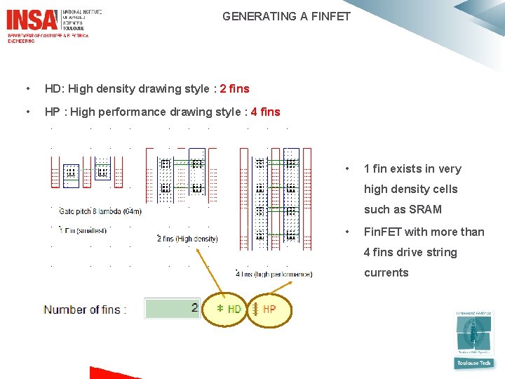
GENERATING A FINFET • HD: High density drawing style : 2 fins • HP : High performance drawing style : 4 fins • 1 fin exists in very high density cells such as SRAM • Fin. FET with more than 4 fins drive string currents

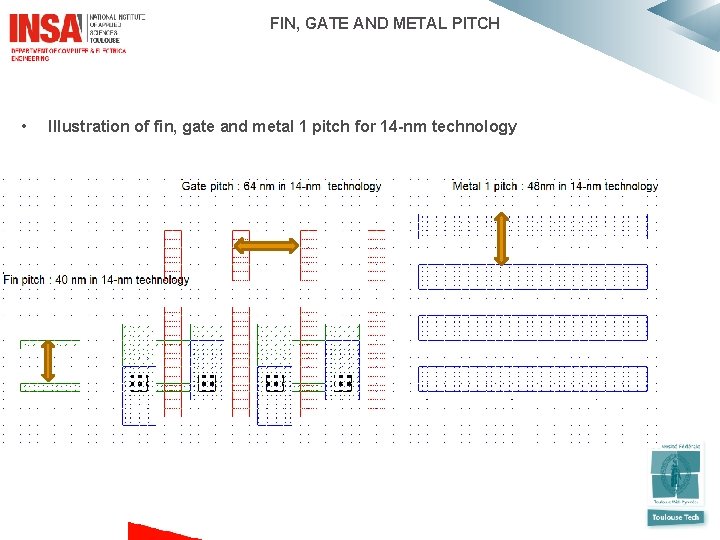
FIN, GATE AND METAL PITCH • Illustration of fin, gate and metal 1 pitch for 14 -nm technology

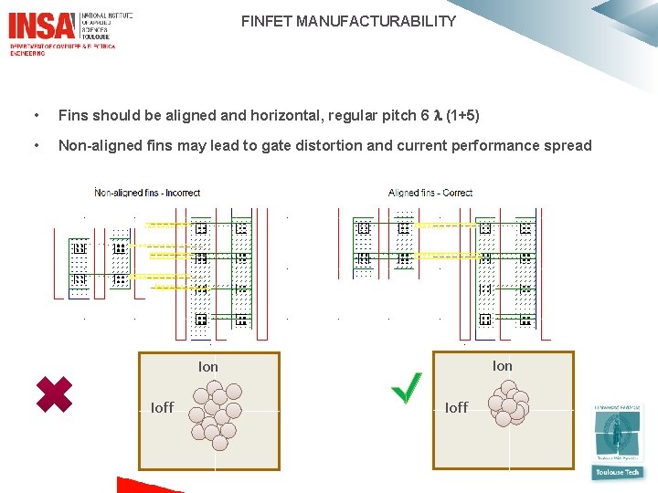
FINFET MANUFACTURABILITY • Fins should be aligned and horizontal, regular pitch 6 (1+5) • Non-aligned fins may lead to gate distortion and current performance spread Ion Ioff

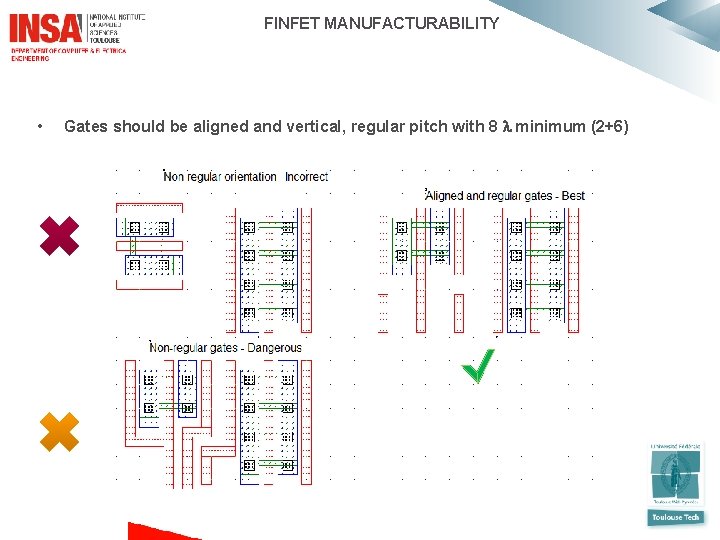
FINFET MANUFACTURABILITY • Gates should be aligned and vertical, regular pitch with 8 minimum (2+6)

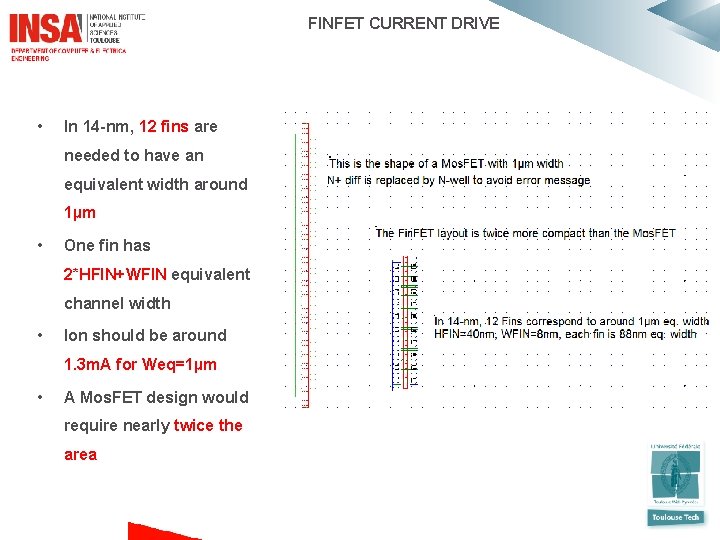
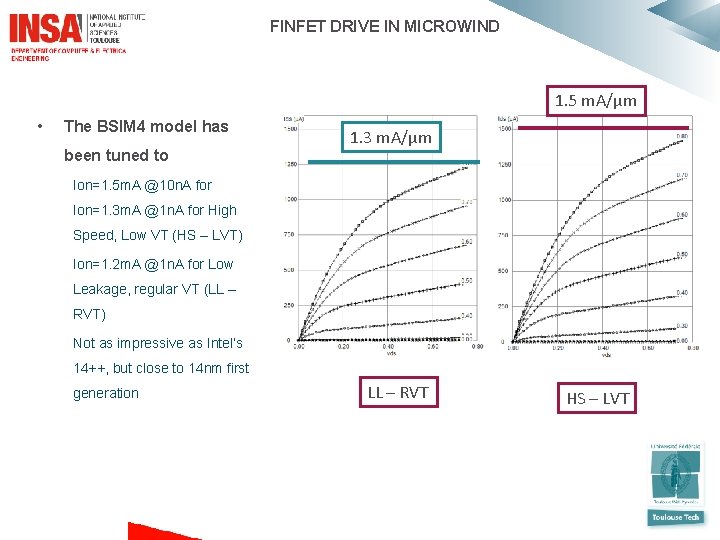
FINFET CURRENT DRIVE • In 14 -nm, 12 fins are needed to have an equivalent width around 1µm • One fin has 2*HFIN+WFIN equivalent channel width • Ion should be around 1. 3 m. A for Weq=1µm • A Mos. FET design would require nearly twice the area

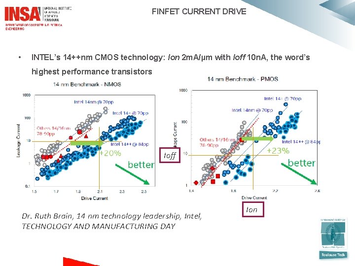
FINFET CURRENT DRIVE • INTEL’s 14++nm CMOS technology: Ion 2 m. A/µm with Ioff 10 n. A, the word’s highest performance transistors Ioff Dr. Ruth Brain, 14 nm technology leadership, Intel, TECHNOLOGY AND MANUFACTURING DAY Ion

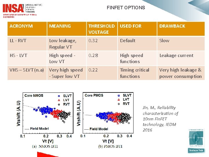
FINFET OPTIONS ACRONYM MEANING THRESHOLD USED FOR VOLTAGE DRAWBACK LL - RVT Low leakage, Regular VT 0. 32 Default Slow HS - LVT High speed - Low VT 0. 28 High speed functions Leakage current Timing critical functions Very high leakage & power consumption VHS – SLVT (n. a) Very high speed 0. 22 - Super low VT Jin, M. , Reliability characterization of 10 nm Fin. FET technology, IEDM 2016

FINFET DRIVE IN MICROWIND 1. 5 m. A/µm • The BSIM 4 model has been tuned to 1. 3 m. A/µm Ion=1. 5 m. A @10 n. A for Ion=1. 3 m. A @1 n. A for High Speed, Low VT (HS – LVT) Ion=1. 2 m. A @1 n. A for Low Leakage, regular VT (LL – RVT) Not as impressive as Intel’s 14++, but close to 14 nm first generation LL – RVT HS – LVT

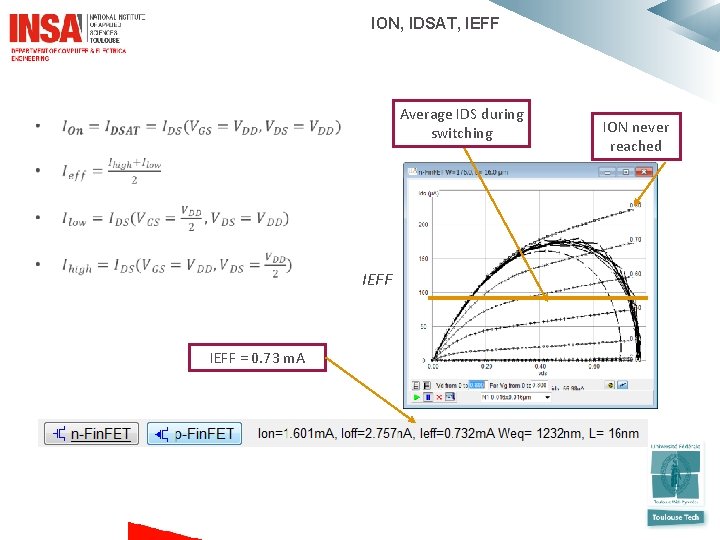
ION, IDSAT, IEFF • Average IDS during switching IEFF = 0. 73 m. A ION never reached

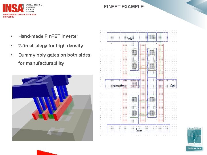
FINFET EXAMPLE • Hand-made Fin. FET inverter • 2 -fin strategy for high density • Dummy poly gates on both sides for manufacturability

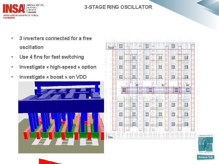
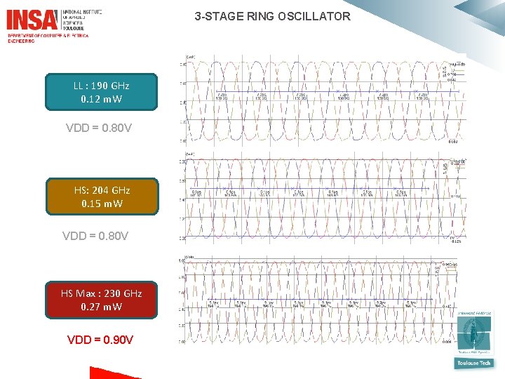
3 -STAGE RING OSCILLATOR • 3 inverters connected for a free oscillation • Use 4 fins for fast switching • Investigate « high-speed » option • Investigate « boost » on VDD

3 -STAGE RING OSCILLATOR LL : 190 GHz 0. 12 m. W VDD = 0. 80 V HS: 204 GHz 0. 15 m. W VDD = 0. 80 V HS Max : 230 GHz 0. 27 m. W VDD = 0. 90 V

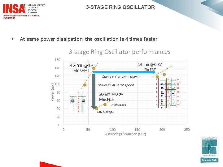
3 -STAGE RING OSCILLATOR At same power dissipation, the oscillation is 4 times faster 3 -stage Ring Oscillator performances 160 14 -nm @0. 8 V Fin. FET 45 -nm @1 V Mos. FET 140 120 Power (µw) • Speed x 4 at same power 100 Power /3 at same speed 80 20 -nm @0. 9 V Mos. FET 60 High speed 40 Low leakage 20 0 0 50 100 150 Oscillating Frequency (GHz) 200 250

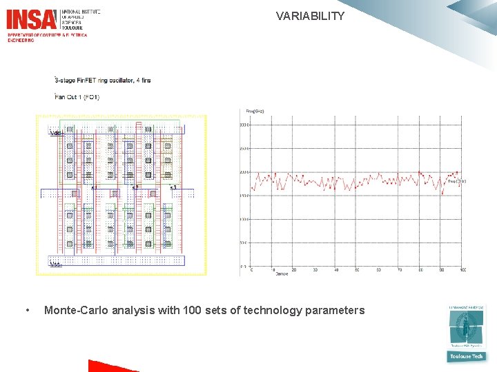
VARIABILITY • Monte-Carlo analysis with 100 sets of technology parameters

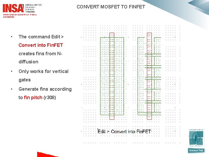
CONVERT MOSFET TO FINFET • The command Edit > Convert into Fin. FET creates fins from Ndiffusion • Only works for vertical gates • Generate fins according to fin pitch (r 308)

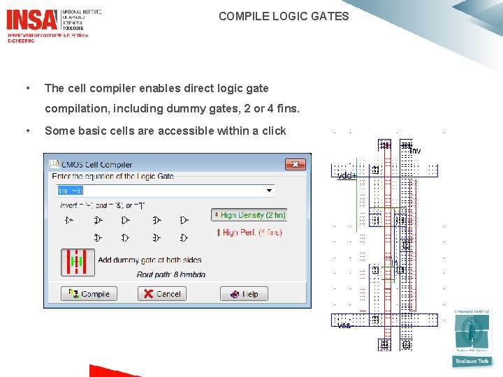
COMPILE LOGIC GATES • The cell compiler enables direct logic gate compilation, including dummy gates, 2 or 4 fins. • Some basic cells are accessible within a click

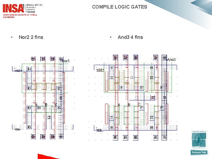
COMPILE LOGIC GATES • Nor 2 2 fins • And 3 4 fins

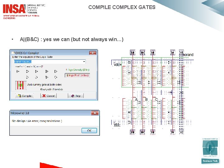
COMPILE COMPLEX GATES • A|(B&C) : yes we can (but not always win…)

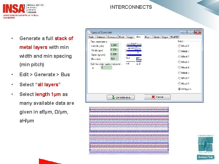
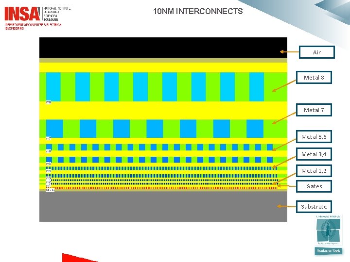
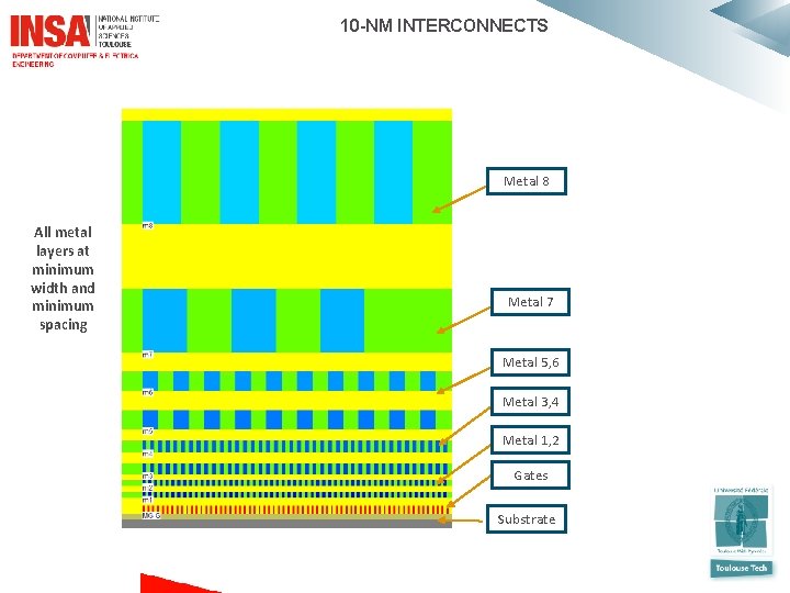
INTERCONNECTS • Generate a full stack of metal layers with min width and min spacing (min pitch) • Edit > Generate > Bus • Select “all layers” • Select length 1µm as many available data are given in af/µm, Ω/µm, a. H/µm

10 NM INTERCONNECTS Air Metal 8 Metal 7 Metal 5, 6 Metal 3, 4 Metal 1, 2 Gates Substrate

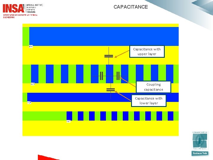
CAPACITANCE Capacitance with upper layer Coupling capacitance Capacitance with lower layer

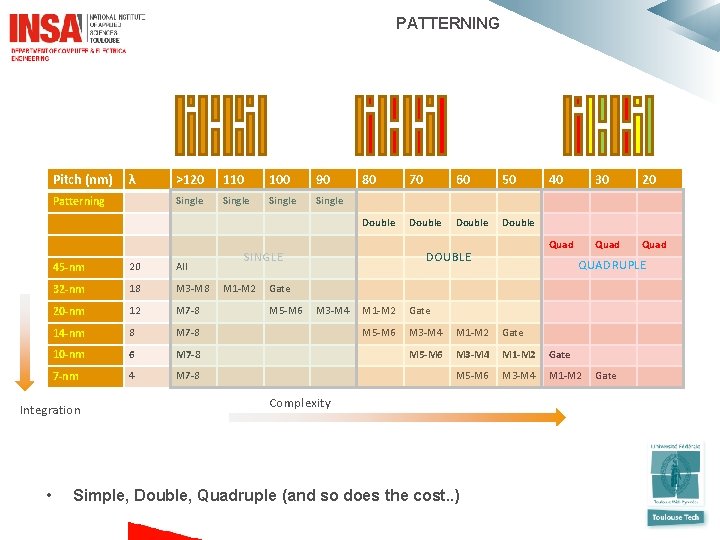
PATTERNING Pitch (nm) λ Patterning 110 100 90 Single 45 -nm 20 All 32 -nm 18 M 3 -M 8 20 -nm 12 M 7 -8 14 -nm 8 M 7 -8 10 -nm 6 M 7 -8 7 -nm 4 M 7 -8 Integration • >120 80 70 60 50 Double SINGLE M 1 -M 2 DOUBLE 40 30 20 Quad QUADRUPLE Gate M 5 -M 6 M 3 -M 4 M 1 -M 2 Complexity Simple, Double, Quadruple (and so does the cost. . ) Gate

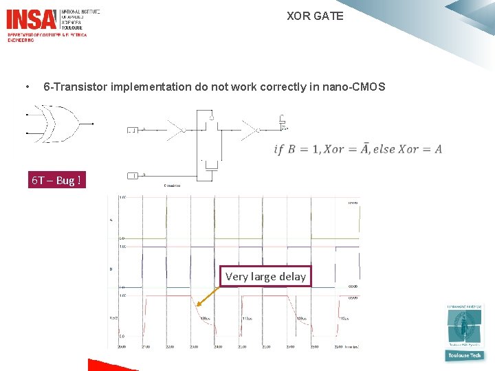
XOR GATE • 6 -Transistor implementation do not work correctly in nano-CMOS 6 T – Bug ! Very large delay

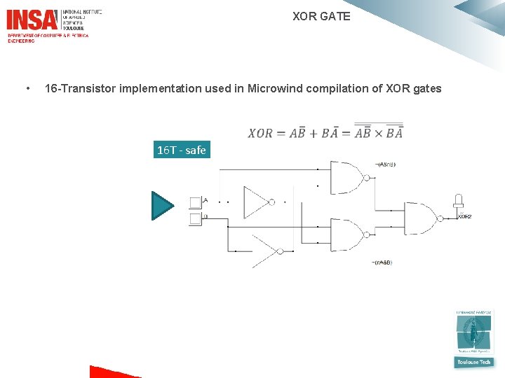
XOR GATE • 16 -Transistor implementation used in Microwind compilation of XOR gates 16 T - safe

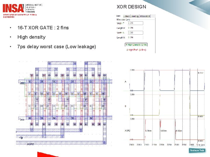
XOR DESIGN • 16 -T XOR GATE : 2 fins • High density • 7 ps delay worst case (Low leakage)

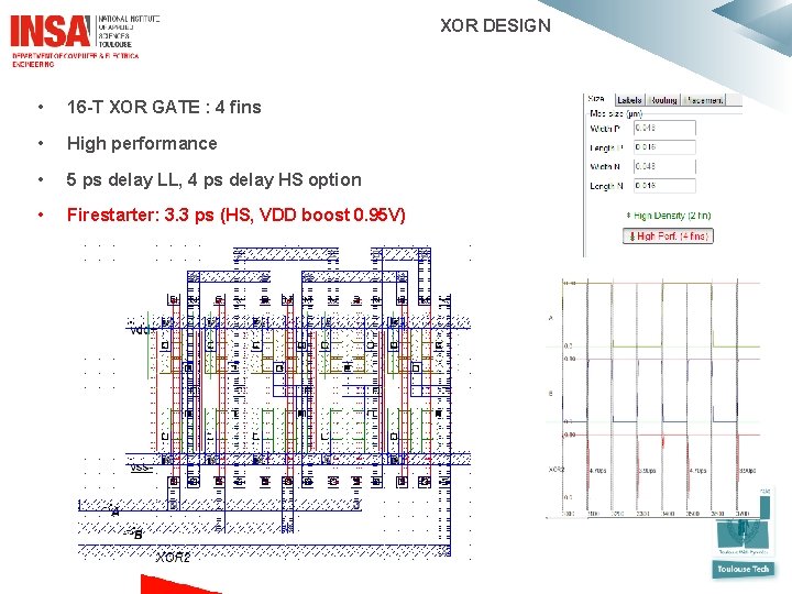
XOR DESIGN • 16 -T XOR GATE : 4 fins • High performance • 5 ps delay LL, 4 ps delay HS option • Firestarter: 3. 3 ps (HS, VDD boost 0. 95 V)

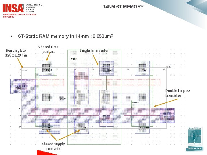
14 NM 6 T MEMORY • 6 T-Static RAM memory in 14 -nm : 0. 050µm 2 Bonding box 328 x 129 nm Shared Data contact Single fin inverter Double fin pass transistor Shared supply contacts

10 NM FINFET IN MICROWIND DEPARTMENT OF ELECTRICAL & COMPUTER ENGINEERING

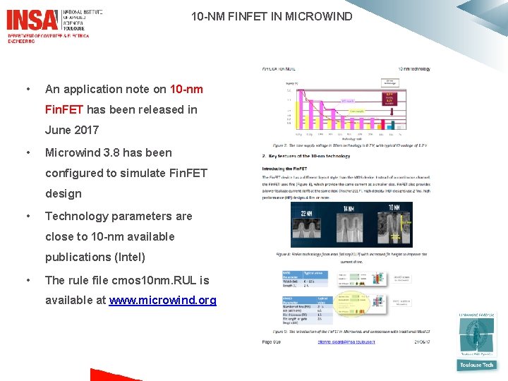
10 -NM FINFET IN MICROWIND • An application note on 10 -nm Fin. FET has been released in June 2017 • Microwind 3. 8 has been configured to simulate Fin. FET design • Technology parameters are close to 10 -nm available publications (Intel) • The rule file cmos 10 nm. RUL is available at www. microwind. org

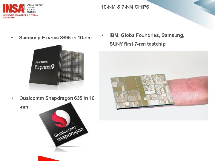
10 -NM & 7 -NM CHIPS • Samsung Exynos 8895 in 10 -nm • IBM, Global. Foundries, Samsung, SUNY first 7 -nm testchip • Qualcomm Snapdragon 635 in 10 -nm

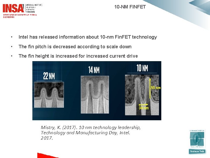
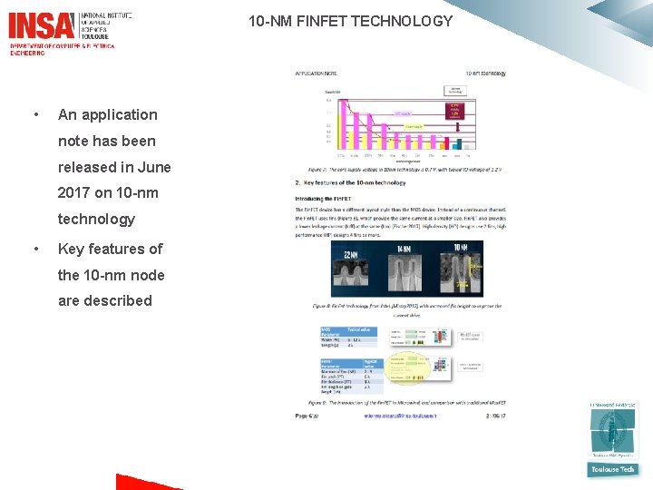
10 -NM FINFET • Intel has released information about 10 -nm Fin. FET technology • The fin pitch is decreased according to scale down • The fin height is increased for increased current drive Mistry, K. (2017). 10 nm technology leadership, Technology and Manufacturing Day, Intel. 2017.

10 -NM FINFET TECHNOLOGY • An application note has been released in June 2017 on 10 -nm technology • Key features of the 10 -nm node are described

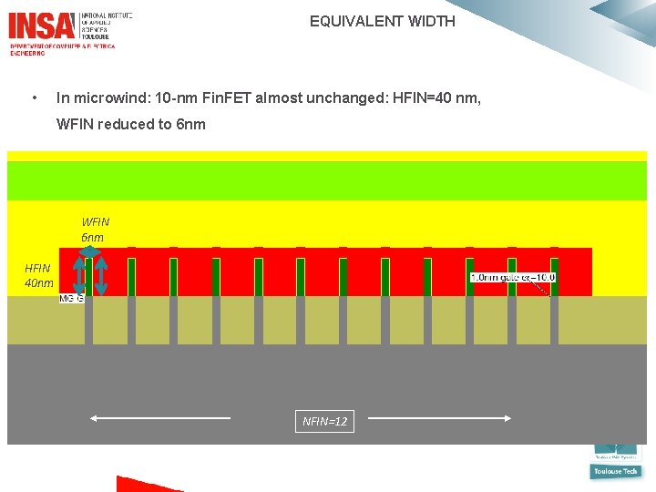
EQUIVALENT WIDTH • In microwind: 10 -nm Fin. FET almost unchanged: HFIN=40 nm, WFIN reduced to 6 nm WFIN 6 nm HFIN 40 nm NFIN=12

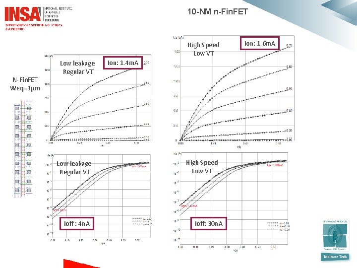
10 -NM n-Fin. FET High Speed Low VT N-Fin. FET Weq=1µm Low leakage Regular VT Ioff : 4 n. A Ion: 1. 4 m. A High Speed Low VT Ioff: 30 n. A Ion: 1. 6 m. A

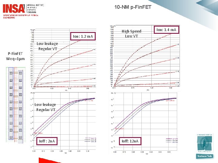
10 -NM p-Fin. FET Ion: 1. 2 m. A P-Fin. FET Weq=1µm High Speed Low VT Low leakage Regular VT Ioff : 2 n. A Ioff: 12 n. A Ion: 1. 4 m. A

10 -NM INTERCONNECTS Metal 8 All metal layers at minimum width and minimum spacing Metal 7 Metal 5, 6 Metal 3, 4 Metal 1, 2 Gates Substrate

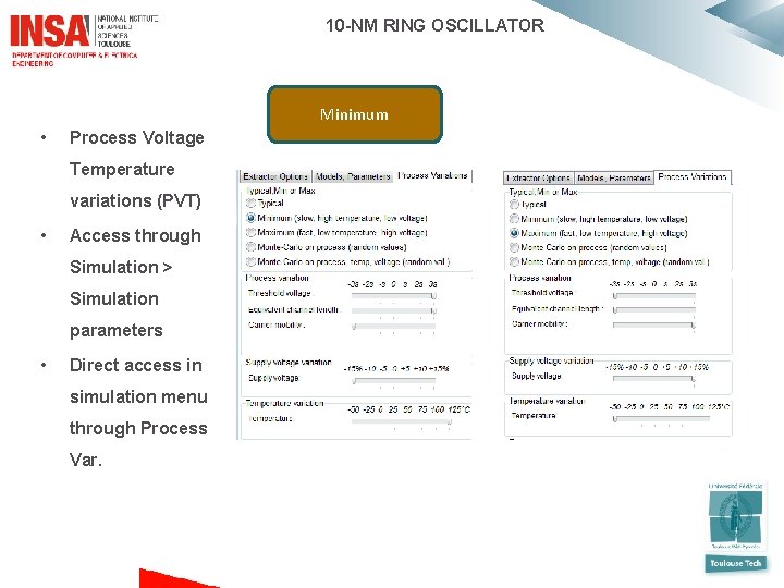
10 -NM RING OSCILLATOR Minimum • Process Voltage Temperature variations (PVT) • Access through Simulation > Simulation parameters • Direct access in simulation menu through Process Var.

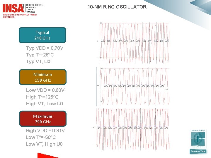
10 -NM RING OSCILLATOR Typical 240 GHz Typ VDD = 0. 70 V Typ T°=25°C Typ VT, U 0 Minimum 150 GHz Low VDD = 0. 60 V High T°=125°C High VT, Low U 0 Maximum 290 GHz High VDD = 0. 81 V Low T°=-50°C Low VT, High U 0

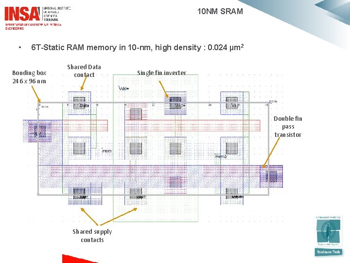
10 NM SRAM • 6 T-Static RAM memory in 10 -nm, high density : 0. 024 µm 2 Bonding box 246 x 96 nm Shared Data contact Single fin inverter Double fin pass transistor Shared supply contacts

7 NM FINFET IN MICROWIND DEPARTMENT OF ELECTRICAL & COMPUTER ENGINEERING

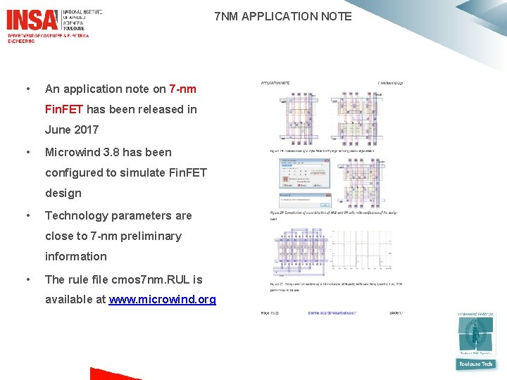
7 NM APPLICATION NOTE • An application note on 7 -nm Fin. FET has been released in June 2017 • Microwind 3. 8 has been configured to simulate Fin. FET design • Technology parameters are close to 7 -nm preliminary information • The rule file cmos 7 nm. RUL is available at www. microwind. org

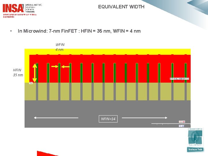
EQUIVALENT WIDTH • In Microwind: 7 -nm Fin. FET : HFIN = 35 nm, WFIN = 4 nm WFIN 4 nm HFIN 35 nm NFIN=14

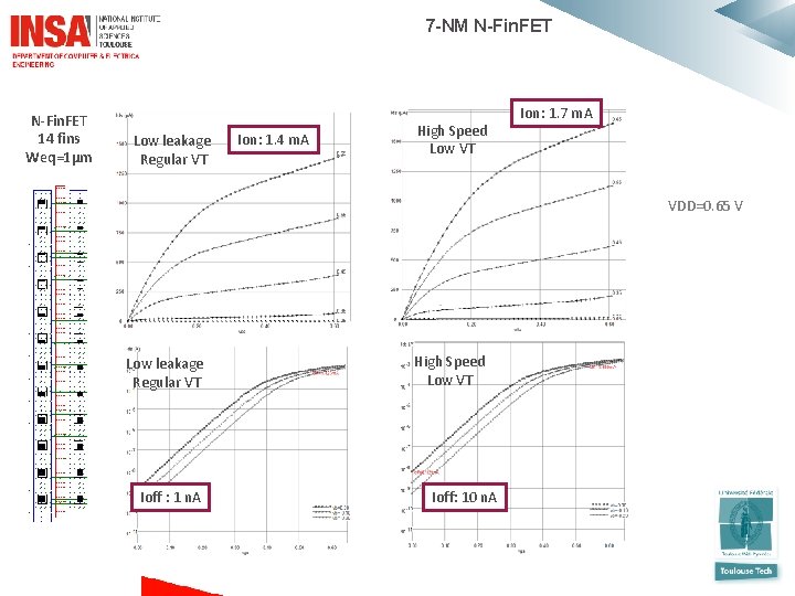
7 -NM N-Fin. FET 14 fins Weq=1µm Low leakage Regular VT Ion: 1. 4 m. A High Speed Low VT Ion: 1. 7 m. A VDD=0. 65 V Low leakage Regular VT Ioff : 1 n. A High Speed Low VT Ioff: 10 n. A

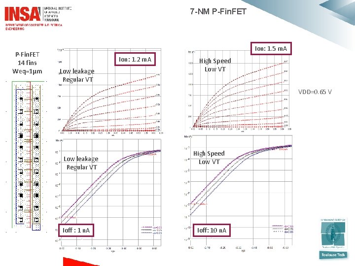
7 -NM P-Fin. FET 14 fins Weq=1µm Ion: 1. 5 m. A Ion: 1. 2 m. A Low leakage Regular VT High Speed Low VT VDD=0. 65 V Low leakage Regular VT Ioff : 1 n. A High Speed Low VT Ioff: 10 n. A

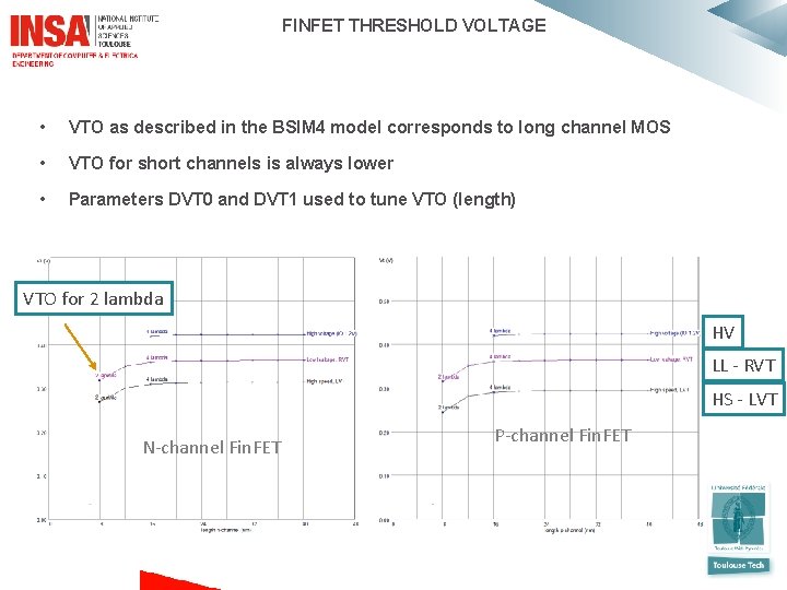
FINFET THRESHOLD VOLTAGE • VTO as described in the BSIM 4 model corresponds to long channel MOS • VTO for short channels is always lower • Parameters DVT 0 and DVT 1 used to tune VTO (length) VTO for 2 lambda HV LL - RVT HS - LVT N-channel Fin. FET P-channel Fin. FET

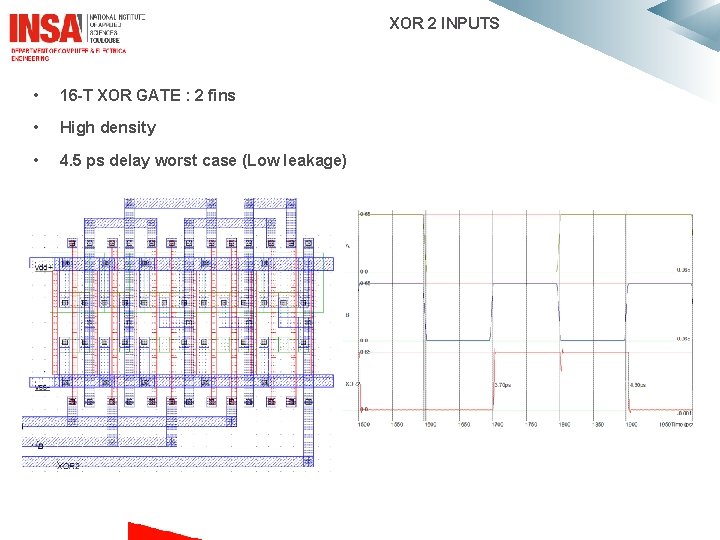
XOR 2 INPUTS • 16 -T XOR GATE : 2 fins • High density • 4. 5 ps delay worst case (Low leakage)

10 -NM RING OSCILLATOR Typical 240 GHz Typ VDD = 0. 70 V Typ T°=25°C Typ VT, U 0 Minimum 150 GHz Low VDD = 0. 60 V High T°=125°C High VT, Low U 0 Maximum 290 GHz High VDD = 0. 81 V Low T°=-50°C Low VT, High U 0

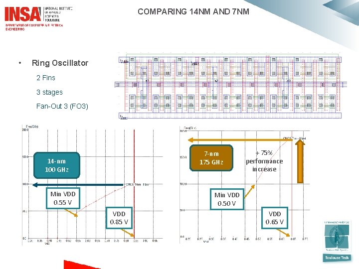
COMPARING 14 NM AND 7 NM • Ring Oscillator 2 Fins 3 stages Fan-Out 3 (FO 3) 7 -nm 175 GHz 14 -nm 100 GHz Min VDD 0. 55 V + 75% performance increase Min VDD 0. 50 V VDD 0. 85 V VDD 0. 65 V

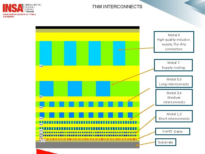
7 NM INTERCONNECTS Metal 8 High quality inductor, supply, flip chip connection Metal 7 Supply routing Metal 5, 6 Long interconnects Metal 3, 4 Medium interconnects Metal 1, 2 Short interconnects Fin. FET Gates Substrate

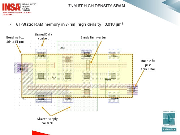
7 NM 6 T HIGH DENSITY SRAM • 6 T-Static RAM memory in 7 -nm, high density : 0. 010 µm 2 Bonding box 164 x 64 nm Shared Data contact Single fin inverter Double fin pass transistor Shared supply contacts

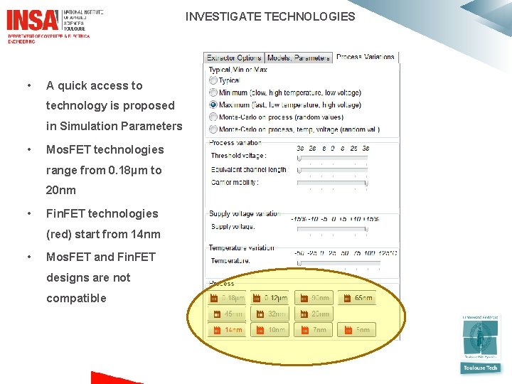
INVESTIGATE TECHNOLOGIES • A quick access to technology is proposed in Simulation Parameters • Mos. FET technologies range from 0. 18µm to 20 nm • Fin. FET technologies (red) start from 14 nm • Mos. FET and Fin. FET designs are not compatible