
12 BIT 500 MHz ADC Module for the
12 -BIT, 500 MHz ADC Module for the KOTO Experiment The University of Chicago Mircea Bogdan 1
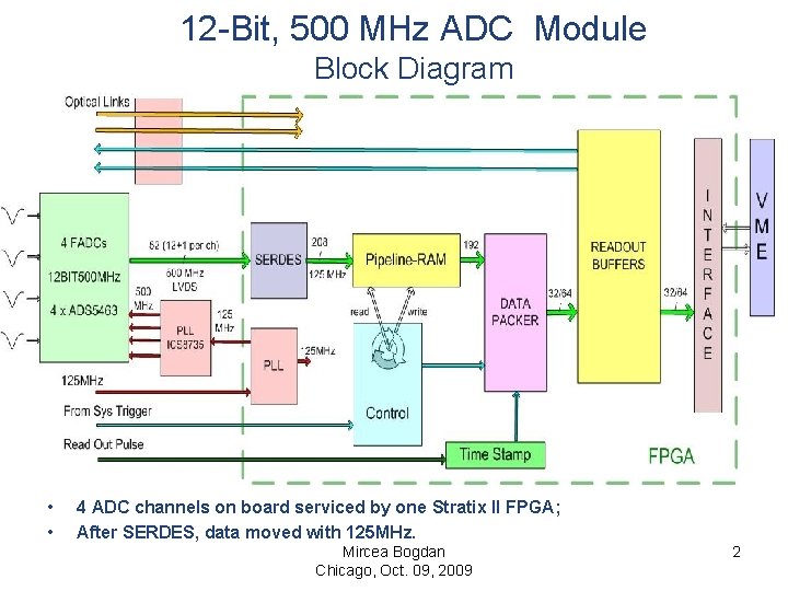
12 -Bit, 500 MHz ADC Module Block Diagram • • 4 ADC channels on board serviced by one Stratix II FPGA; After SERDES, data moved with 125 MHz. Mircea Bogdan Chicago, Oct. 09, 2009 2
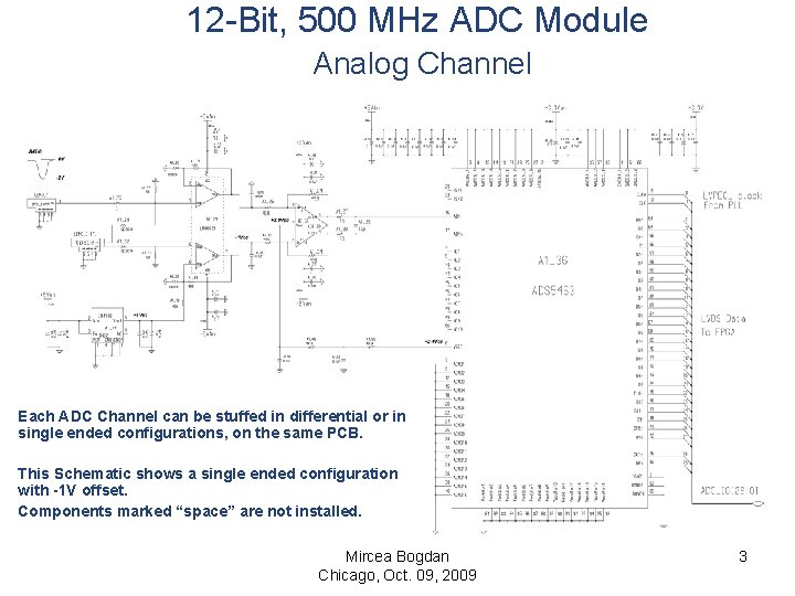
12 -Bit, 500 MHz ADC Module Analog Channel Each ADC Channel can be stuffed in differential or in single ended configurations, on the same PCB. This Schematic shows a single ended configuration with -1 V offset. Components marked “space” are not installed. Mircea Bogdan Chicago, Oct. 09, 2009 3

12 -Bit, 500 MHz ADC Module Specifications • 4 Channel, 12 -BIT, 500 MSPS ADC: – ADS 5463 by TI; • • 6 U VME 64 x; Front Panel LVDS I/Os: – RJ 45 (same as the 14 -BIT ADC): • 3 Inputs; • 1 Output; – 0. 1” Right Angle Header: Insert 4 ADC • 4 Inputs; • 4 Outputs; • Channels in this Area. Front Panel LVTTL I/Os: – 8 I/Os configurable; • Front Panel Optical I/Os: – 2 Inputs 2. 5 to 3. 125 Gbps; – 2 Output 2. 5 to 3. 125 Gbps; Old 14 -BIT, 125 MSPS ADC: Mircea Bogdan Chicago, Oct. 09, 2009 4
12 -Bit, 500 MHz FADC Module Conclusions The Digital part of the 4 -Channel 500 MSPS Module is very similar to the 16 - Channel 125 MSPS Module. Many Logical Blocks will be reused in this new design. Design process as short as possible. Mircea Bogdan Chicago, Oct. 09, 2009 5
- Slides: 5