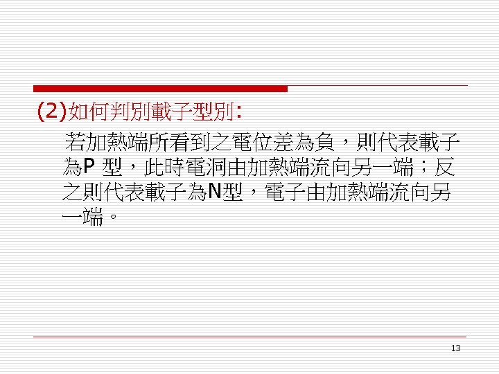
100 WAFER 111 is an natural etching stop
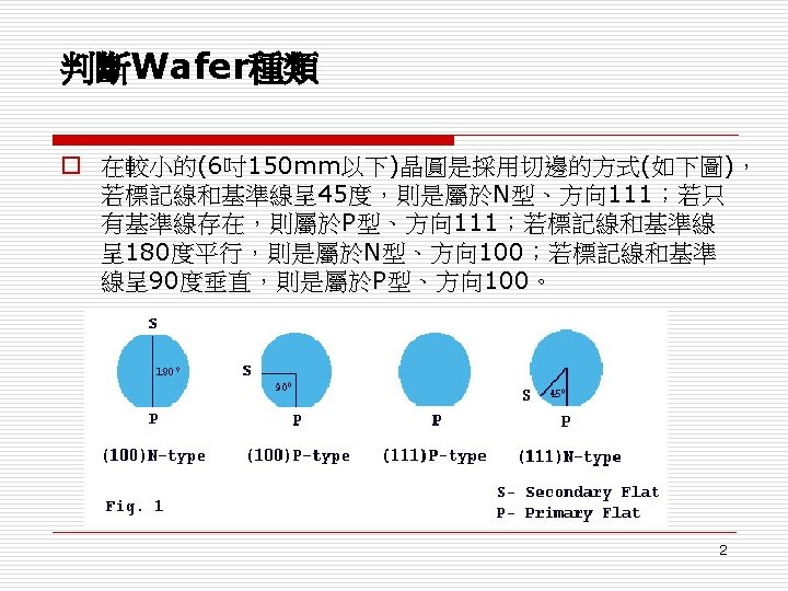
 WAFER {111} is an natural etching stop plane and cut plane Yu-Shiang Huang")
 異丙醇(IPA) 去離子水(DI water) BOE 去離子水(DI 去除native water)oxide (~1 nm)")


- Slides: 17
(100) WAFER {111} is an natural etching stop plane and cut plane Yu-Shiang Huang et al. , VLSI 2019, pp T 180~T 181. 3
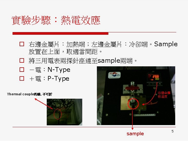
清洗晶片 丙酮去除有機物 震洗去除particles o 丙酮(ACE) 異丙醇(IPA) 去離子水(DI water) BOE 去離子水(DI 去除native water)oxide (~1 nm) o 用氮氣吹乾時應保持sample固定 o Si wafer hydrophobic (疏水) o Native oxide (~1 nm) hydrophilic (親水) M. Morita et al. , JAP, 1990 4
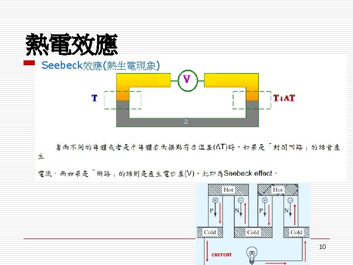
Ø 實驗數據 Group 1 -3 Hot 40 50. 1 60 70. 1 Cool 28. 4 29. 5 30. 9 32. 3 Group 1 -2 ΔV(m V) 11. 6 12. 2 20. 6 18 29. 1 26 37. 8 33. 2 ΔT(℃) Hot 39. 9 50 59. 9 70 Cool 28. 8 30. 3 31. 5 32. 1 ΔV(m. V ) 11. 1 8. 6 19. 7 16. 1 28. 4 22. 8 37. 9 31. 6 ΔT(℃) Group 1 -1 Hot 39. 9 50. 2 60. 2 70. 1 Cool 26. 9 28. 1 29. 6 30. 9 ΔV(m V) 13 -5. 1 22. 1 -8. 2 30. 6 -11. 1 39. 2 -14. 9 ΔT(℃) 7
BACKUP 9
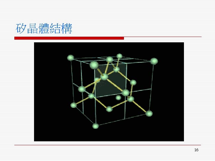
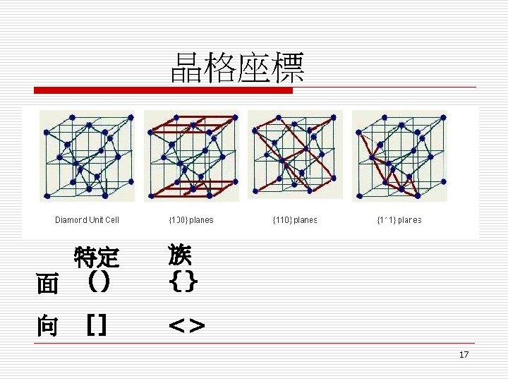
結報問題 1. Look up for HF toxicity and safety issues from MSDS. What should be done in case of contact? How should HF be recycled? 2. What are PEL-TWA, PEL-STEL, and PEL-C? 3. What are the applications of thermoelectric effect? 4. Check out the 18 -inch wafer in EE 2 -220. 5. Please draw the diamond structure, and list at least 5 materials with the diamond structure. 6. For (100), (110), and (111) Si, what are the orientations of fracture plane (斷裂面) and the directions along fraction plane? 15