10 Memory Hierarchy Design Kai Bu kaibuzju edu

10 Memory Hierarchy Design Kai Bu kaibu@zju. edu. cn http: //list. zju. edu. cn/kaibu/comparch 2018
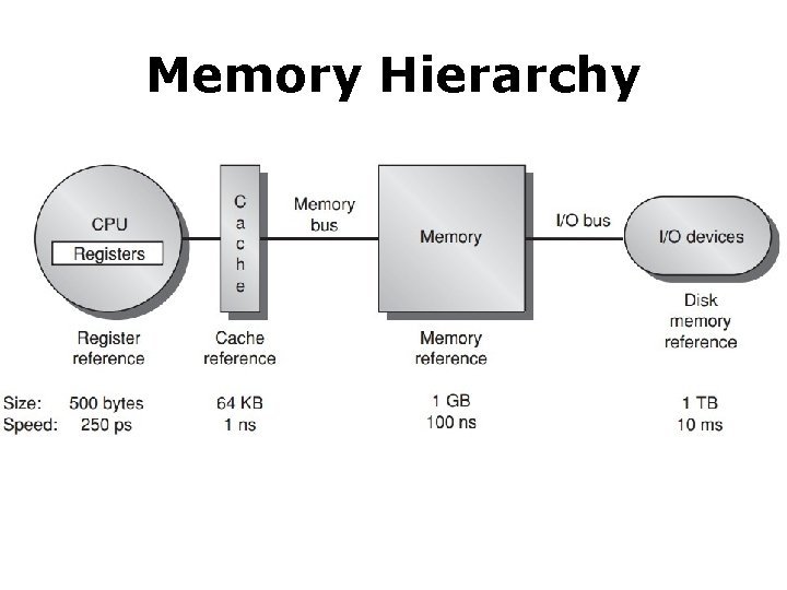
Memory Hierarchy
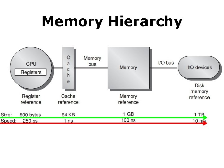
Memory Hierarchy
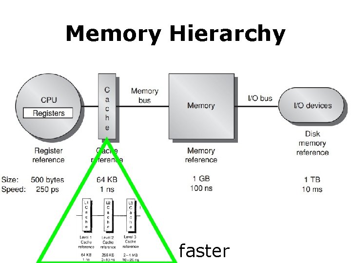
Memory Hierarchy faster
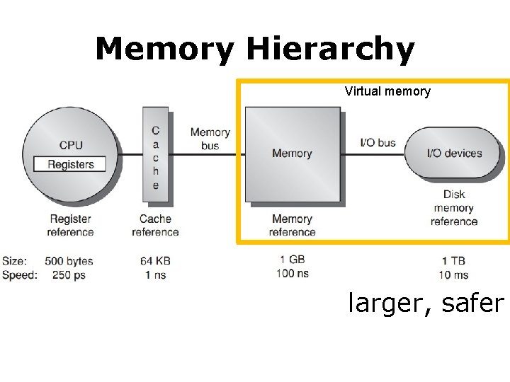
Memory Hierarchy Virtual memory larger, safer

I know how they work, basically…

They should work better?

They should work better? toward optimization!

They should work better? toward optimization?
Preview • How to optimize cache? • How to optimize memory?
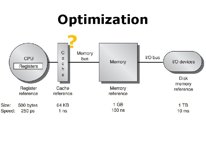
Optimization ?
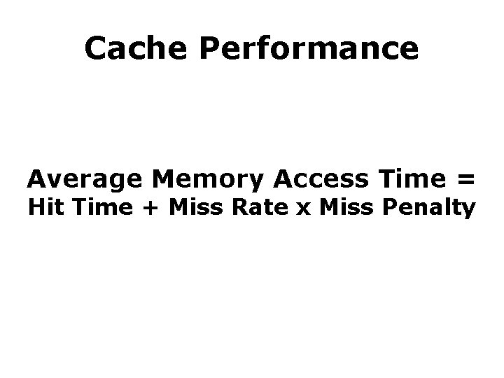
Cache Performance Average Memory Access Time = Hit Time + Miss Rate x Miss Penalty
six basic optimizations
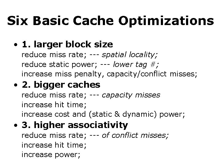
Six Basic Cache Optimizations • 1. larger block size reduce miss rate; --- spatial locality; reduce static power; --- lower tag #; increase miss penalty, capacity/conflict misses; • 2. bigger caches reduce miss rate; --- capacity misses increase hit time; increase cost and (static & dynamic) power; • 3. higher associativity reduce miss rate; --- of conflict misses; increase hit time; increase power;
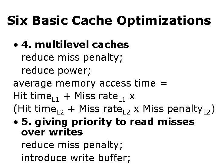
Six Basic Cache Optimizations • 4. multilevel caches reduce miss penalty; reduce power; average memory access time = Hit time. L 1 + Miss rate. L 1 x (Hit time. L 2 + Miss rate. L 2 x Miss penalty. L 2) • 5. giving priority to read misses over writes reduce miss penalty; introduce write buffer;
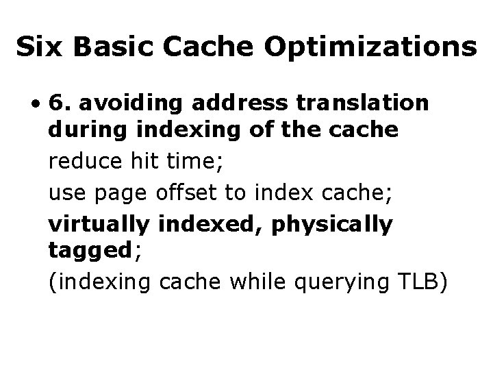
Six Basic Cache Optimizations • 6. avoiding address translation during indexing of the cache reduce hit time; use page offset to index cache; virtually indexed, physically tagged; (indexing cache while querying TLB)
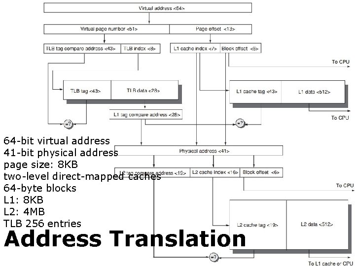
64 -bit virtual address 41 -bit physical address page size: 8 KB two-level direct-mapped caches 64 -byte blocks L 1: 8 KB L 2: 4 MB TLB 256 entries Address Translation
ten advanced optimizations
Ten Advanced Cache Opts • Goal: average memory access time • Metrics to reduce/optimize hit time miss rate miss penalty cache bandwidth power consumption
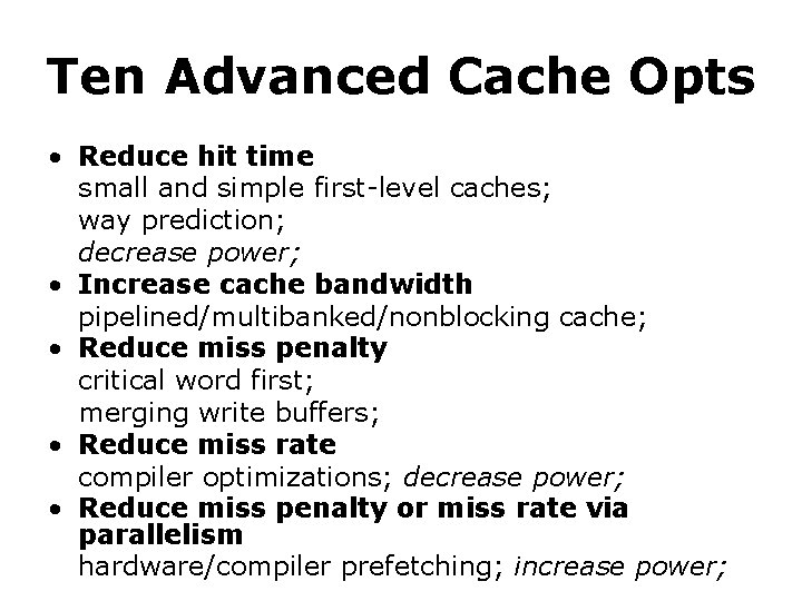
Ten Advanced Cache Opts • Reduce hit time small and simple first-level caches; way prediction; decrease power; • Increase cache bandwidth pipelined/multibanked/nonblocking cache; • Reduce miss penalty critical word first; merging write buffers; • Reduce miss rate compiler optimizations; decrease power; • Reduce miss penalty or miss rate via parallelism hardware/compiler prefetching; increase power;
Opt #1: Small and Simple First -Level Caches • Small size support a fast clock cycle reduce power • Lower associativity reduce both hit time and power (direct-mapped caches can overlap the tag check with the transmission of the data)
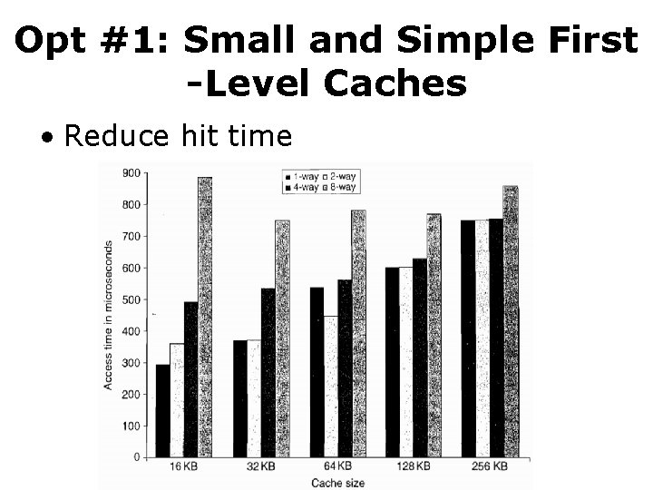
Opt #1: Small and Simple First -Level Caches • Reduce hit time
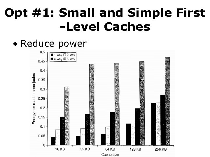
Opt #1: Small and Simple First -Level Caches • Reduce power
Opt #2: Way Prediction • Reduce conflict misses and hit time • Way prediction block predictor bits are added to each block to predict the way/block within the set of the next cache access the multiplexor is set early to select the desired block; only a single tag comparison is performed in parallel with cache reading; a miss results in checking the other blocks for matches in the next clock cycle;
Opt #3: Pipelined Cache Access • Increase cache bandwidth • Higher latency • Greater penalty on mispredicted branches and more clock cycles between issuing the load and using the data
Opt #4: Nonblocking Caches • Increase cache bandwidth • Nonblocking/lockup-free cache leverage out-of-order execution allows data cache to continue to supply cache hits during a miss;
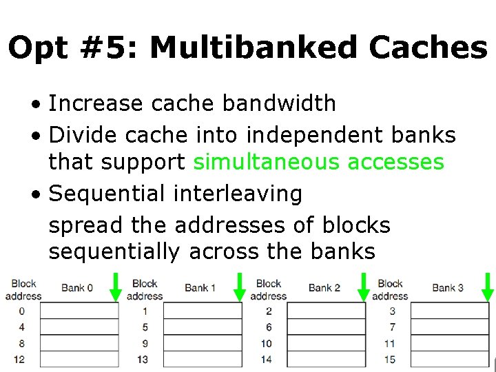
Opt #5: Multibanked Caches • Increase cache bandwidth • Divide cache into independent banks that support simultaneous accesses • Sequential interleaving spread the addresses of blocks sequentially across the banks
Opt #6: Critical Word First & Early Restart • Reduce miss penalty • Motivation: the processor normally needs just one word of the block at a time • Critical word first request the missed word first from the memory and send it to the processor as soon as it arrives; processor continues execution while filling the rest of the words in the block • Early restart fetch the words in normal order, as soon as the requested word arrives send it to the processor;
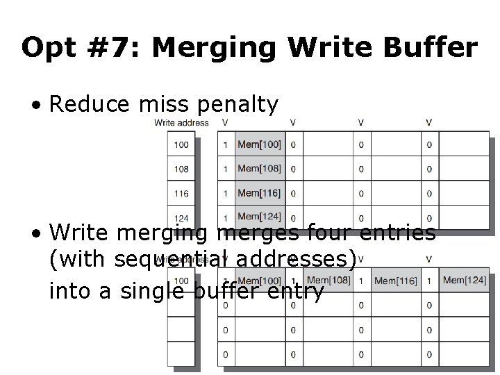
Opt #7: Merging Write Buffer • Reduce miss penalty • Write merging merges four entries (with sequential addresses) into a single buffer entry
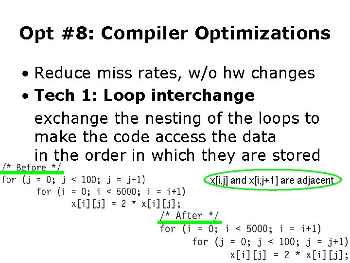
Opt #8: Compiler Optimizations • Reduce miss rates, w/o hw changes • Tech 1: Loop interchange exchange the nesting of the loops to make the code access the data in the order in which they are stored x[i, j] and x[i, j+1] are adjacent
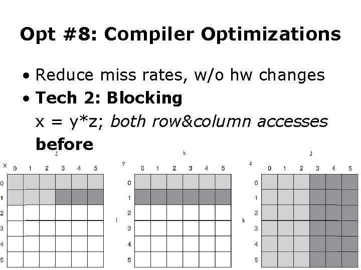
Opt #8: Compiler Optimizations • Reduce miss rates, w/o hw changes • Tech 2: Blocking x = y*z; both row&column accesses before x
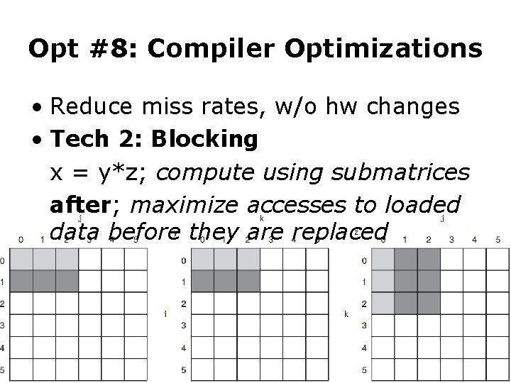
Opt #8: Compiler Optimizations • Reduce miss rates, w/o hw changes • Tech 2: Blocking x = y*z; compute using submatrices after; maximize accesses to loaded data before they are replaced
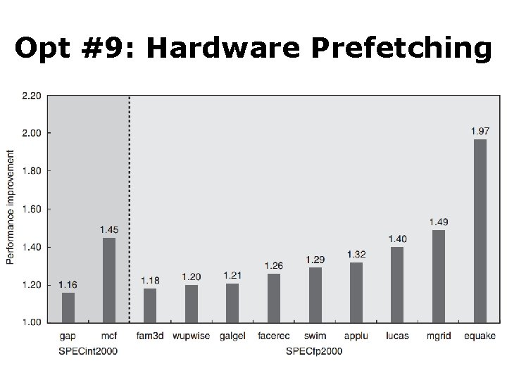
Opt #9: Hardware Prefetching • Reduce miss penalty/rate • Prefetch items before the processor requests them, into the cache or external buffer • Instruction prefetch two blocks on a miss: requested one into cache + next consecutive one into instruction stream buffer • Similar Data prefetch approaches
Opt #9: Hardware Prefetching
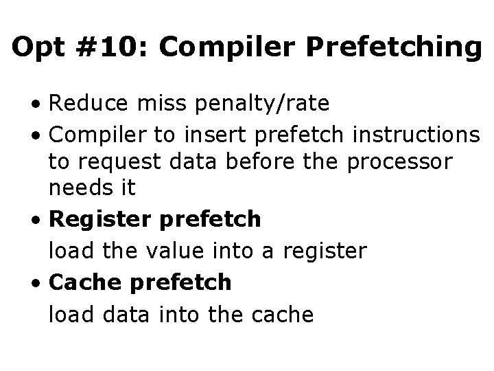
Opt #10: Compiler Prefetching • Reduce miss penalty/rate • Compiler to insert prefetch instructions to request data before the processor needs it • Register prefetch load the value into a register • Cache prefetch load data into the cache
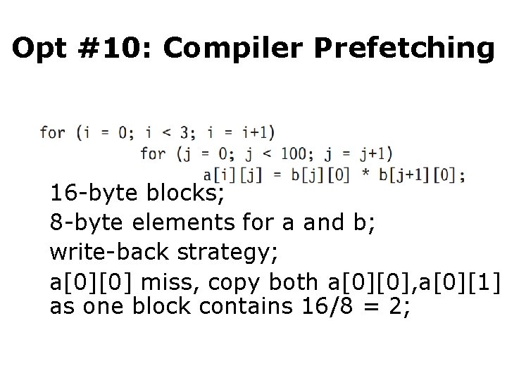
Opt #10: Compiler Prefetching • Example: 251 misses 16 -byte blocks; 8 -byte elements for a and b; write-back strategy; a[0][0] miss, copy both a[0][0], a[0][1] as one block contains 16/8 = 2; so for a: 3 x (100/2) = 150 misses b[0][0] – b[100][0]: 101 misses
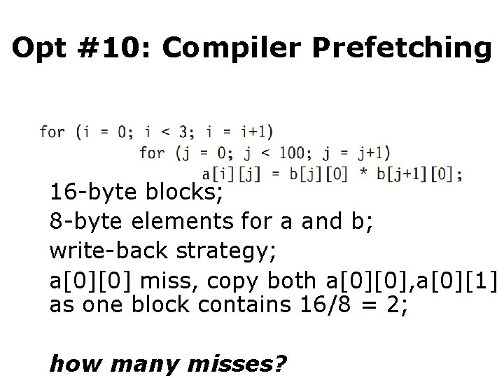
Opt #10: Compiler Prefetching • Example: 251 misses 16 -byte blocks; 8 -byte elements for a and b; write-back strategy; a[0][0] miss, copy both a[0][0], a[0][1] as one block contains 16/8 = 2; how many misses?

Opt #10: Compiler Prefetching • Example: 251 misses 16 -byte blocks; 8 -byte elements for a and b; write-back strategy; a[0][0] miss, copy both a[0][0], a[0][1] as one block contains 16/8 = 2; so for a: 3 x (100/2) = 150 misses b[0][0] – b[100][0]: 101 misses
![Opt #10: Compiler Prefetching • Example: 19 ? misses by prefetching 7 misses: b[0][0] Opt #10: Compiler Prefetching • Example: 19 ? misses by prefetching 7 misses: b[0][0]](http://slidetodoc.com/presentation_image_h/06386cf6fb10bfb39c38cccd7b4b8efa/image-39.jpg)
Opt #10: Compiler Prefetching • Example: 19 ? misses by prefetching 7 misses: b[0][0] – b[6][0] 4 misses: 1/2 of a[0][0] – a[0][6] 4 misses: a[1][0] – a[1][6] 4 misses: a[2][0] – a[2][6]
![Opt #10: Compiler Prefetching • Example: 19 misses by prefetching 7 misses: b[0][0] – Opt #10: Compiler Prefetching • Example: 19 misses by prefetching 7 misses: b[0][0] –](http://slidetodoc.com/presentation_image_h/06386cf6fb10bfb39c38cccd7b4b8efa/image-40.jpg)
Opt #10: Compiler Prefetching • Example: 19 misses by prefetching 7 misses: b[0][0] – b[6][0] 4 misses: 1/2 of a[0][0] – a[0][6] 4 misses: a[1][0] – a[1][6] 4 misses: a[2][0] – a[2][6]
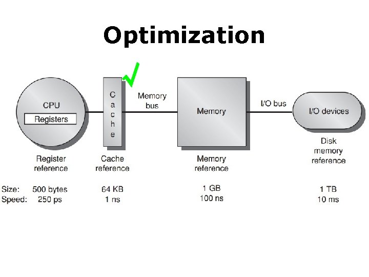
Optimization √
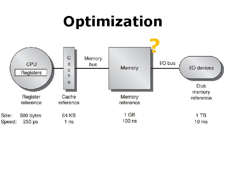
Optimization ?
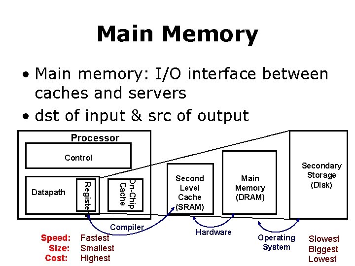
Main Memory • Main memory: I/O interface between caches and servers • dst of input & src of output Processor Control On-Chip Cache Registers Datapath Compiler Speed: Size: Cost: Fastest Smallest Highest Second Level Cache (SRAM) Hardware Main Memory (DRAM) Operating System Secondary Storage (Disk) Slowest Biggest Lowest
Main Memory Performance measures • Latency the time to retrieve the first word of the block important for caches; harder to reduce; • Bandwidth the time to retrieve the rest of this block important for multiprocessors, I/O, and caches with large block sizes; easier to improve with new organizations;
Main Memory Performance measures • Latency access time: the time between when a read is requested and when the desired word arrives; cycle time: the minimum time between unrelated requests to memory; or the minimum time between the start of an access and the start of the next access;
Main Memory • SRAM for cache • DRAM for main memory
SRAM • Static Random Access Memory • Six transistors per bit to prevent the information from being disturbed when read • Don’t need to refresh, so access time is very close to cycle time
DRAM • Dynamic Random Access Memory • Single transistor per bit • Reading destroys the information • Refresh periodically • cycle time > access time
DRAM • Dynamic Random Access Memory • Single transistor per bit • Reading destroys the information • Refresh periodically • cycle time > access time DRAMs are commonly sold on small boards called DIMM (dual inline memory modules), typically containing 4 ~ 16 DRAMs
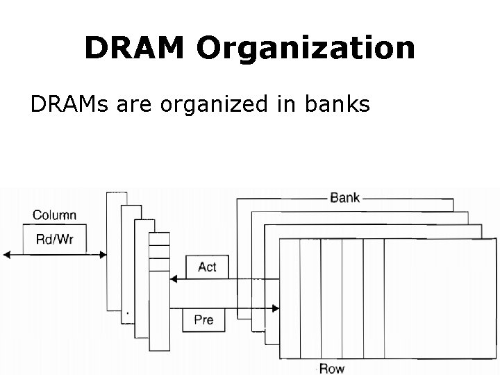
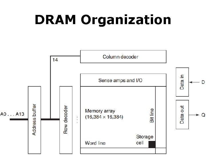
DRAM Organization DRAMs are organized in banks
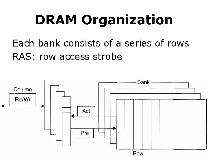
DRAM Organization Each bank consists of a series of rows RAS: row access strobe
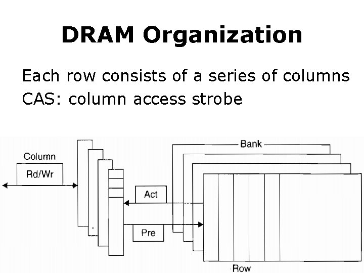
DRAM Organization Each row consists of a series of columns CAS: column access strobe
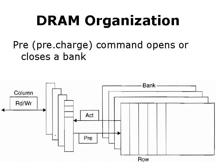
DRAM Organization Pre (pre. charge) command opens or closes a bank
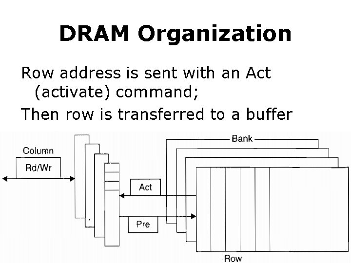
DRAM Organization Row address is sent with an Act (activate) command; Then row is transferred to a buffer
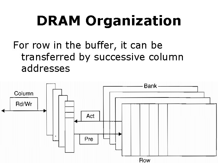
DRAM Organization For row in the buffer, it can be transferred by successive column addresses
DRAM Organization
DRAM Improvement • Timing signals allow repeated accesses to the row buffer w/o another row access time; • Leverage spatial locality each array will buffer 1024 to 4096 bits for each access;
DRAM Improvement • Clock signal added to the DRAM interface, so that repeated transfers will not involve overhead to synchronize with memory controller; • SDRAM: synchronous DRAM
DRAM Improvement • Wider DRAM to overcome the problem of getting a wide stream of bits from memory without having to make the memory system too large as memory system density increased; widening the cache and memory widens memory bandwidth; e. g. , 4 -bit transfer mode up to 16 -bit buses
DRAM Improvement • DDR: double data rate to increase bandwidth, transfer data on both the rising edge and falling edge of the DRAM clock signal, thereby doubling the peak data rate;
DRAM Improvement • Multiple Banks break a single SDRAM into 2 to 8 blocks; they can operate independently; • Provide some of the advantages of interleaving • Help with power management
DRAM Improvement • Reducing power consumption in SDRAMs dynamic power: used in a read or write; static/standby power • Depend on the operating voltage • Power down mode: entered by telling the DRAM to ignore the clock disables the SDRAM except for internal
Flash Memory • A type of EEPROM (electronically erasable programmable read-only memory) • Read-only but can be erased • Hold contents w/o any power
Flash Memory Differences from DRAM • Must be erased (in blocks) before it is overwritten • Static and less power consumption • Has a limited number of write cycles for any block • Cheaper than SDRAM but more expensive than disk • Slower than SDRAM but faster than disk
Memory Dependability • Soft errors changes to a cell’s contents, not a change in the circuitry • Hard errors permanent changes in the operation of one or more memory cells
Memory Dependability Error detection and fix • Parity only one bit of overhead to detect a single error in a sequence of bits; e. g. , one parity bit per 8 data bits • ECC only detect two errors and correct a single error with 8 -bit overhead per 64 data bits • Chipkill handle multiple errors and complete failure of a single memory chip
Memory Dependability Rates of unrecoverable errors in 3 yrs • Parity only about 90, 000, or one unrecoverable (undetected) failure every 17 mins • ECC only about 3, 500 or about one undetected or unrecoverable failure every 7. 5 hrs • Chipkill 6, or about one undetected or unrecoverable failure every 2 months
Virtual Memory • The architecture must limit what a process can access when running a user process yet allow an OS process to access more • Four tasks for the architecture
Virtual Memory • Task 1 The architecture provides at least two modes, indicating whether the running process is a user process or an OS process (kernel/supervisor process)
Virtual Memory • Task 2 The architecture provides a portion of the processor state that a user process can use but not write
Virtual Memory • Task 3 The architecture provides mechanisms whereby the processor can go from user mode to supervisor mode (system call) and vice versa
Virtual Memory • Task 4 The architecture provides mechanisms to limit memory accesses to protect the memory state of a process w/o having to swap the process to disk on a context switch
Virtual Machines • Virtual Machine a protection mode with a much smaller code base than the full OS • VMM: virtual machine monitor hypervisor software that supports VMs • Host underlying hardware platform
Virtual Machines • Requirements 1. Guest software should behave on a VM exactly as if it were running on the native hardware 2. Guest software should not be able to change allocation of real system resources directly
VMM: Virtual Machine Monitor • three essential characteristics: 1. VMM provides an environment for programs which is essentially identical with the original machine; 2. programs run in this environment show at worst only minor decreases in speed; 3. VMM is in complete control of system resources; • Mainly for security and privacy sharing and protection among multiple processes

Chapter 2 Appendix B
Labs 3 -5 • Lab 3 Demo: December 17, 2018 Report: January 07, 2019 • Lab 4 Demo: December 24, 2018 Report: January 07, 2019 • Lab 5 Demo: January 07, 2019 Report: January 14, 2019


Thank You wherever you go, there you are.

#What’s More • The Ten Suggestions by Ben Bernanke • The Lesson of Grace in Teaching by Francis Su
- Slides: 80