
1 Wideband pulse amplifier for the integrated camera
1 Wideband pulse amplifier for the integrated camera of the Cherenkov Telescope Array E. Delagnesa, A. Sanuyb, D. Gascónb on behalf of the NECTAr collaboration Irfu /CEA/Saclay a LPNHE / Paris LPTA / Montpellier ICC / Universitat Barcelona (ICC-UB) b TWEPP – Aachen – September 21 th 2010
2 Outlook I. Introduction II. Basic building blocks III. First prototype: ACTA IV. Second prototype: ACTA 3 V. Summary
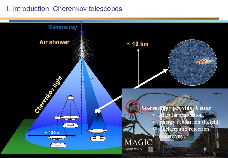
I. Introduction: Cherenkov telescopes Gamma ray Air shower ~ 10 km Ch er en ko vl ig ht ~ 1 o ~ 120 m Stereoscopy provides better: • Angular resolution. • Energy resolution (height). • Background rejection. • Sensitivity.
I. Introduction: the Cherenkov Telescope Array (CTA) observatory How CTA aims to extend energy range and increase sensitivity? Large array (>1 km 2)of Cherenkov telescopes (50 -100) Different sizes: dish from 6 to 24 m Camera and electronics must be optimized in terms of Current Instrumentation Performance Cost and reliability: integration
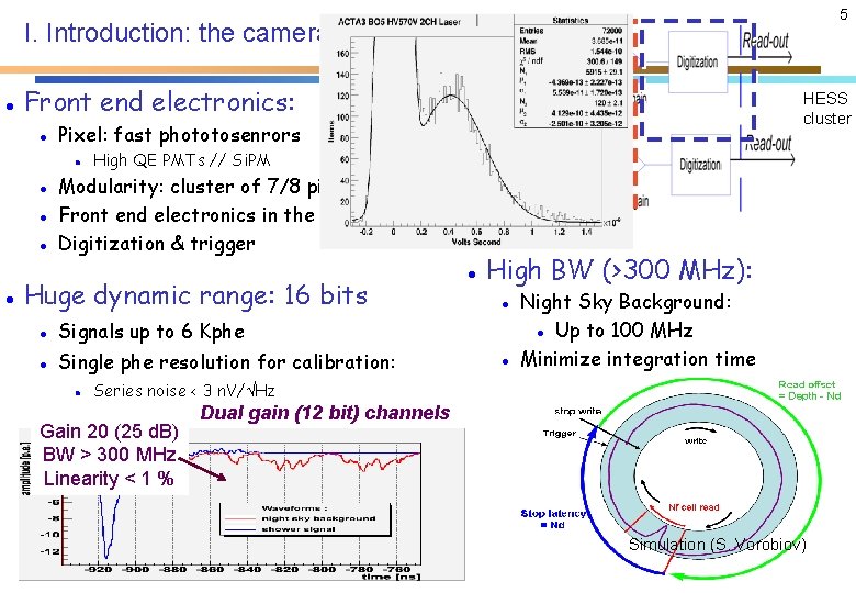
5 I. Introduction: the camera Front end electronics: Pixel: fast phototosenrors HESS cluster High QE PMTs // Si. PM Modularity: cluster of 7/8 pixels Front end electronics in the camera Digitization & trigger Huge dynamic range: 16 bits Signals up to 6 Kphe Single phe resolution for calibration: High BW (>300 MHz): Night Sky Background: Up to 100 MHz Minimize integration time Series noise < 3 n. V/ Hz Gain 20 (25 d. B) BW > 300 MHz Linearity < 1 % Dual gain (12 bit) channels Simulation (S. Vorobiov)
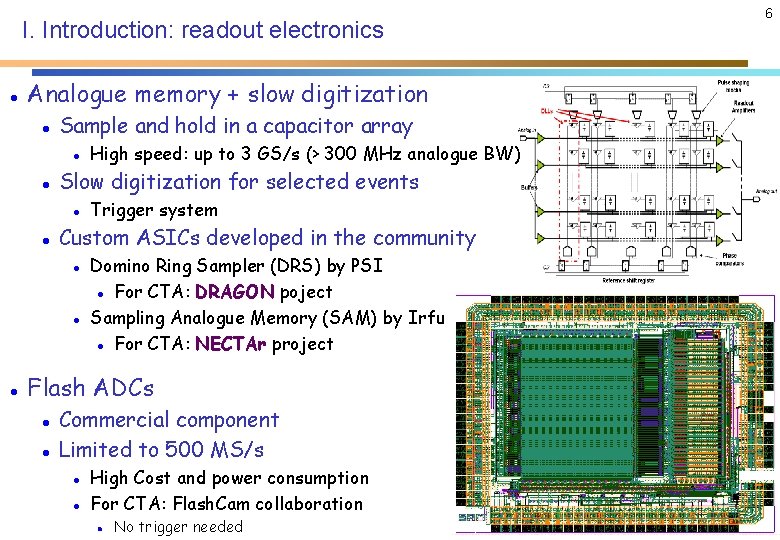
I. Introduction: readout electronics Analogue memory + slow digitization Sample and hold in a capacitor array Slow digitization for selected events Trigger system Custom ASICs developed in the community High speed: up to 3 GS/s (> 300 MHz analogue BW) Domino Ring Sampler (DRS) by PSI For CTA: DRAGON poject Sampling Analogue Memory (SAM) by Irfu For CTA: NECTAr project Flash ADCs Commercial component Limited to 500 MS/s High Cost and power consumption For CTA: Flash. Cam collaboration No trigger needed 6
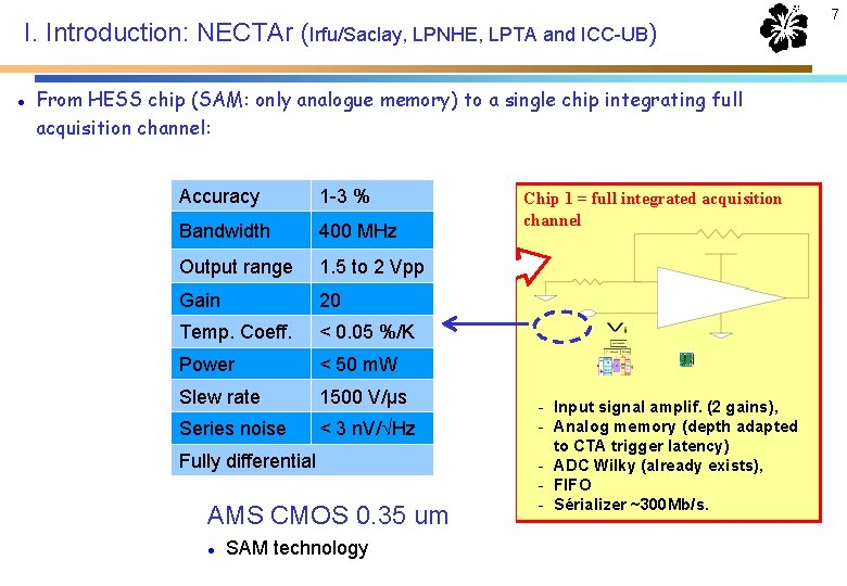
I. Introduction: NECTAr (Irfu/Saclay, LPNHE, LPTA and ICC-UB) From HESS chip (SAM: only analogue memory) to a single chip integrating full acquisition channel: NECTAr chip: COST & RELIABILITY Accuracy 1 -3 % Bandwidth 400 MHz Chip 1 = full integrated acquisition channel FE board HESS-2 Output range 1. 5 to 2 Vpp E. Delagnes Gain 20 Temp. Coeff. < 0. 05 %/K Power < 50 m. W Slew rate 1500 V/µs Series noise < 3 n. V/ Hz Fully differential Chip 2: Integrated local trigger: - 8 or 16 fast comparators. AMS CMOS 0. 35 um - Coincidences in < 1 ns SAM technology - Input signal amplif. (2 gains), - Analog memory (depth adapted to CTA trigger latency) - ADC Wilky (already exists), - FIFO - Sérializer ~300 Mb/s. 7
8 Outlook I. Introduction II. The circuit III. First prototype: ACTA IV. Second prototype: ACTA 3 V. Summary
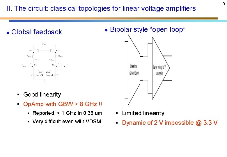
II. The circuit: classical topologies for linear voltage amplifiers Global feedback Bipolar style “open loop” § Good linearity § Op. Amp with GBW > 8 GHz !! § Reported: < 1 GHz in 0. 35 um § Limited linearity § Very difficult even with VDSM § Dynamic of 2 V impossible @ 3. 3 V 9
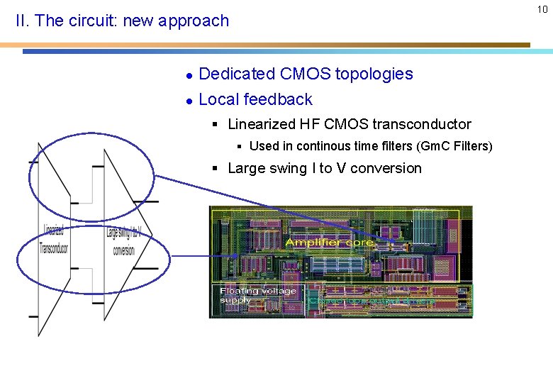
10 II. The circuit: new approach Dedicated CMOS topologies Local feedback § Linearized HF CMOS transconductor § Used in continous time filters (Gm. C Filters) § Large swing I to V conversion
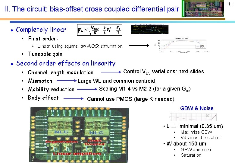
11 II. The circuit: bias-offset cross coupled differential pair Completely linear § First order: • Linear using square law MOS: saturation § Tuneable gain Second order effects on linearity § Channel length modulation Control VDS variations: next slides § Mismatch Large WL and common centroid Scaling M 1 -4 vs M 2 -3 (for a given Gm) § Mobility reduction § Body effect Cannot use PMOS (large K needed) GBW & Noise • L minimal (0. 35 um) • • Maximize GBW Vds must be stable! • W about 150 um • • GBW and noise Saturation
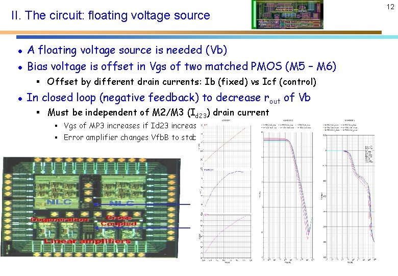
II. The circuit: floating voltage source A floating voltage source is needed (Vb) Bias voltage is offset in Vgs of two matched PMOS (M 5 – M 6) § Offset by different drain currents: Ib (fixed) vs Icf (control) In closed loop (negative feedback) to decrease r out of Vb § Must be independent of M 2/M 3 (Id 23) drain current § Vgs of MP 3 increases if Id 23 increases § Error amplifier changes Vfb. B to stabilize Vb 12
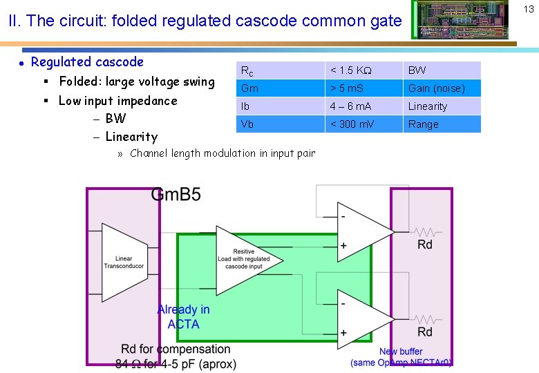
13 II. The circuit: folded regulated cascode common gate Regulated cascode § Folded: large voltage swing § Low input impedance – BW – Linearity RC < 1. 5 K BW Gm > 5 m. S Gain (noise) Ib 4 – 6 m. A Linearity Vb < 300 m. V Range » Channel length modulation in input pair
14 Outlook I. Introduction II. The circuit III. First prototype: ACTA IV. Second prototype: ACTA 3 V. Summary
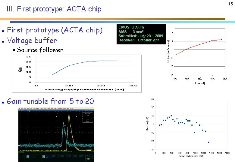
15 III. First prototype: ACTA chip First prototype (ACTA chip) Voltage buffer § Source follower Gain tunable from 5 to 20 CMOS 0. 35 um AMS 3 mm 2 Submitted: July 20 th 2009 Received: October 26 th
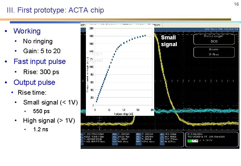
16 III. First prototype: ACTA chip • Working • No ringing • Gain: 5 to 20 • Fast input pulse • Rise: 300 ps • Output pulse • Rise time: • Small signal (< 1 V) • 550 ps • High signal (> 1 V) • 1. 2 ns Small signal Large signal
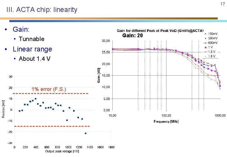
17 III. ACTA chip: linearity • Gain: • Tunnable • Linear range • About 1. 4 V 1% error (F. S. ) Gain: 20
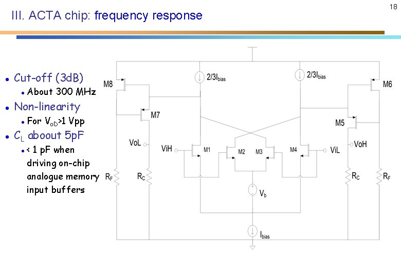
III. ACTA chip: frequency response Cut-off (3 d. B) Non-linearity About 300 MHz For Vo. D>1 Vpp CL aboout 5 p. F < 1 p. F when driving on-chip analogue memory input buffers 18
19 Outlook I. Introduction II. The circuit III. First prototype: ACTA IV. Second prototype: ACTA 3 V. Summary
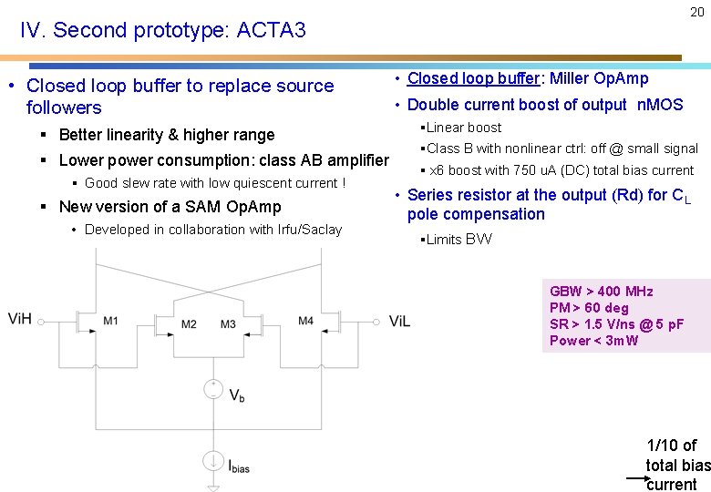
20 IV. Second prototype: ACTA 3 • Closed loop buffer to replace source followers § Better linearity & higher range § Lower power consumption: class AB amplifier § Good slew rate with low quiescent current ! § New version of a SAM Op. Amp • Developed in collaboration with Irfu/Saclay • Closed loop buffer: Miller Op. Amp • Double current boost of output n. MOS § Linear boost § Class B with nonlinear ctrl: off @ small signal § x 6 boost with 750 u. A (DC) total bias current • Series resistor at the output (Rd) for CL pole compensation § Limits BW GBW > 400 MHz PM > 60 deg SR > 1. 5 V/ns @ 5 p. F Power < 3 m. W 1/10 of total bias current
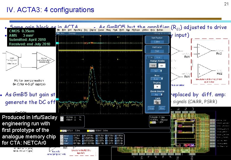
21 IV. ACTA 3: 4 configurations Same gain block as in ACTA to “debug” CMOS 0. 35 um AMS 3 mm 2 Not tested, only Submitted: April 2010 Received: end July 2010 As Gm. BO 5 but the amplifier (Rd 1) adjusted to drive a smaller CL (analogue memory input) As Gm. B 5 but gain stage is modified to generate the DC offset required by ADC Produced in Irfu/Saclay engineering run with first prototype of the analogue memory chip for CTA: NETCAr 0 As Gm. BO 1 but buffer replaced by diff. amp: Subtract common mode signals (CMRR, PSRR)
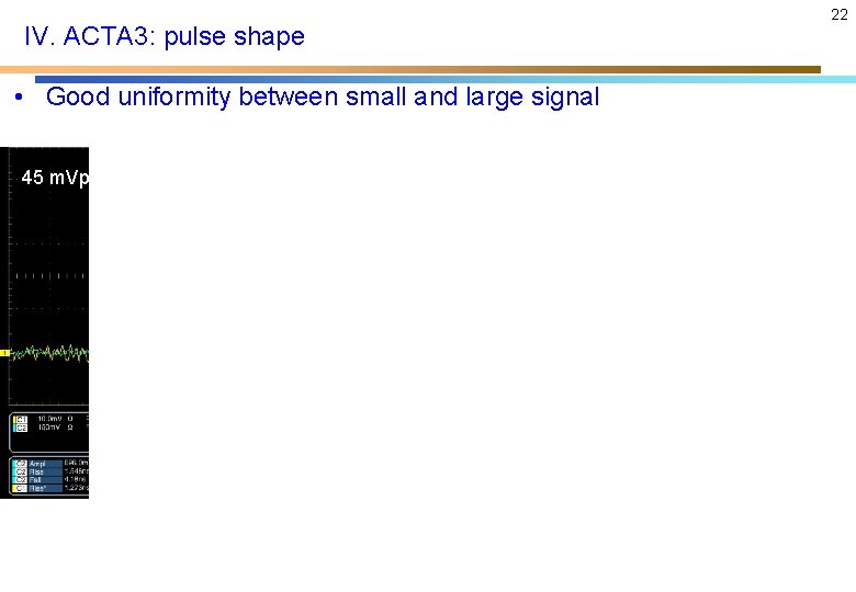
22 IV. ACTA 3: pulse shape • Good uniformity between small and large signal 45 m. Vpp 696 m. Vpp 1. 848 Vpp
IV. ACTA 3: frequency response • Negligible non-linearity performance for Vo. D < 2 Vpp • BW bit smaller than expected (300 MHz): § 250 MHz § BW given by Rd·CL § Underestimation of CL? § Process variation of Rd? 23
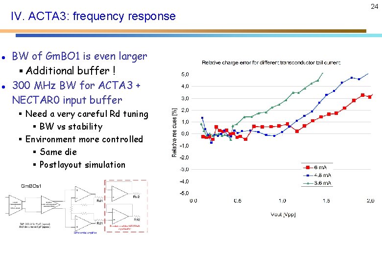
IV. ACTA 3: frequency response BW of Gm. BO 1 is even larger § Additional buffer ! 300 MHz BW for ACTA 3 + NECTAR 0 input buffer § Need a very careful Rd tuning § BW vs stability § Environment more controlled § Same die § Postlayout simulation 24
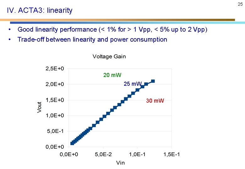
25 IV. ACTA 3: linearity • Good linearity performance (< 1% for > 1 Vpp, < 5% up to 2 Vpp) • Trade-off between linearity and power consumption 20 m. W 25 m. W 30 m. W
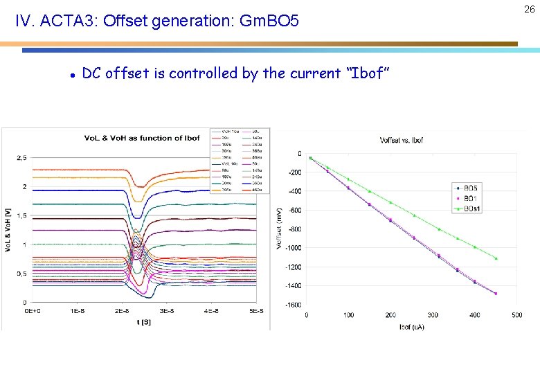
IV. ACTA 3: Offset generation: Gm. BO 5 DC offset is controlled by the current “Ibof” 26
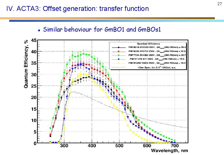
IV. ACTA 3: Offset generation: transfer function Similar behaviour for Gm. BO 1 and Gm. BOs 1 27
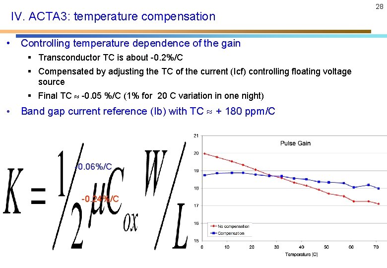
IV. ACTA 3: temperature compensation • Controlling temperature dependence of the gain § Transconductor TC is about -0. 2%/C § Compensated by adjusting the TC of the current (Icf) controlling floating voltage source § Final TC -0. 05 %/C (1% for 20 C variation in one night) • Band gap current reference (Ib) with TC + 180 ppm/C -0. 06%/C -0. 24%/C 28
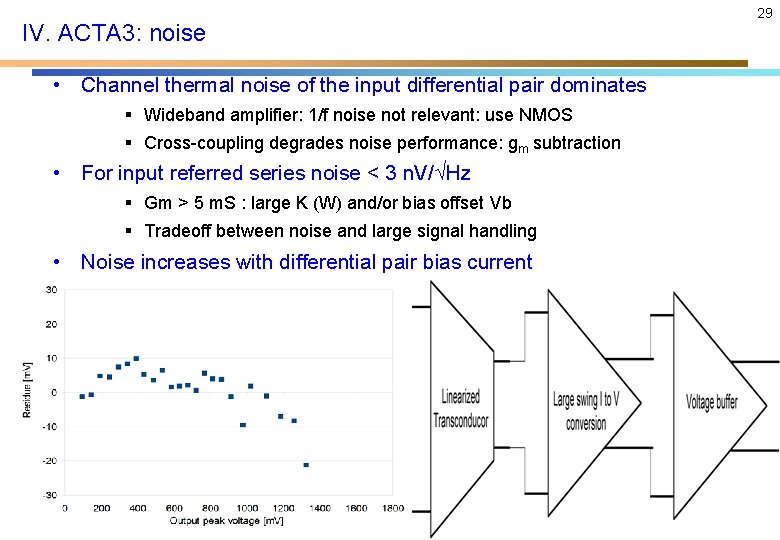
IV. ACTA 3: noise • Channel thermal noise of the input differential pair dominates § Wideband amplifier: 1/f noise not relevant: use NMOS § Cross-coupling degrades noise performance: gm subtraction • For input referred series noise < 3 n. V/ Hz § Gm > 5 m. S : large K (W) and/or bias offset Vb § Tradeoff between noise and large signal handling • Noise increases with differential pair bias current 29
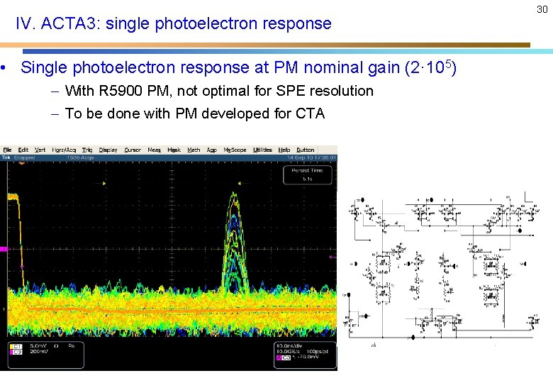
IV. ACTA 3: single photoelectron response • Single photoelectron response at PM nominal gain (2· 105) – With R 5900 PM, not optimal for SPE resolution – To be done with PM developed for CTA 30
31 Outlook I. Introduction II. The circuit III. First prototype: ACTA IV. Second prototype: ACTA 3 V. Summary
32 V. Summary • Alternative solution for wideband pulse amplifiers § Gain: 20 § Bandwidth § > 400 MHz for CL < 1 p. F § > 300 MHz for CL < 5 p. F GBW > 6 GHz in 0. 35 um CMOS technology § Linearity < 1% for 1 Vpp and < 3% for 2 Vpp § For fast “closed loop” amplifiers, linearity is usually limited by slew rate • Intrinsic BW of the core amplifier (without buffer) > 600 MHz § BW > 1 GHz in 130 nm technology ? • Tuneable: § Gain § DC offset : ADC interface § Linearity vs power conssumption

33 Thank you !
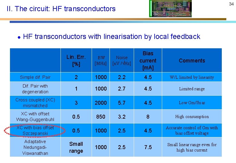
34 II. The circuit: HF transconductors with linearisation by local feedback Lin. Err. [%] BW [MHz] Noise [n. V / Hz] Bias current [m. A] Comments Simple dif. Pair 2 1000 2. 2 4. 5 W/L limited by linearity Dif. Pair with degeneration 1 1000 2. 7 4. 5 Limited range Cross coupled (XC) mismatched 3 2000 5. 7 4. 5 Low Gm/Ibias XC with offset Wang-Guggenbuhl 0. 5 850 3. 2 8 High consumption XC with bias offset Szczepanski 0. 5 1000 2. 5 4. 5 Accurate control of Gm with bias offset voltage Adaptative Nedungadi. Viswanathan Small range 1000 2. 5 7. 5 Small linear range even for high bias current
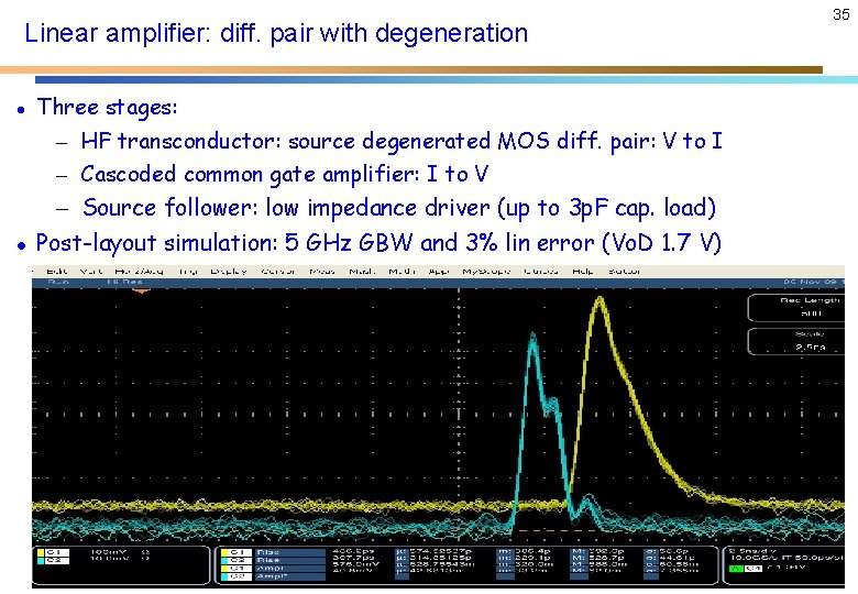
Linear amplifier: diff. pair with degeneration Three stages: – HF transconductor: source degenerated MOS diff. pair: V to I – Cascoded common gate amplifier: I to V – Source follower: low impedance driver (up to 3 p. F cap. load) Post-layout simulation: 5 GHz GBW and 3% lin error (Vo. D 1. 7 V) 35
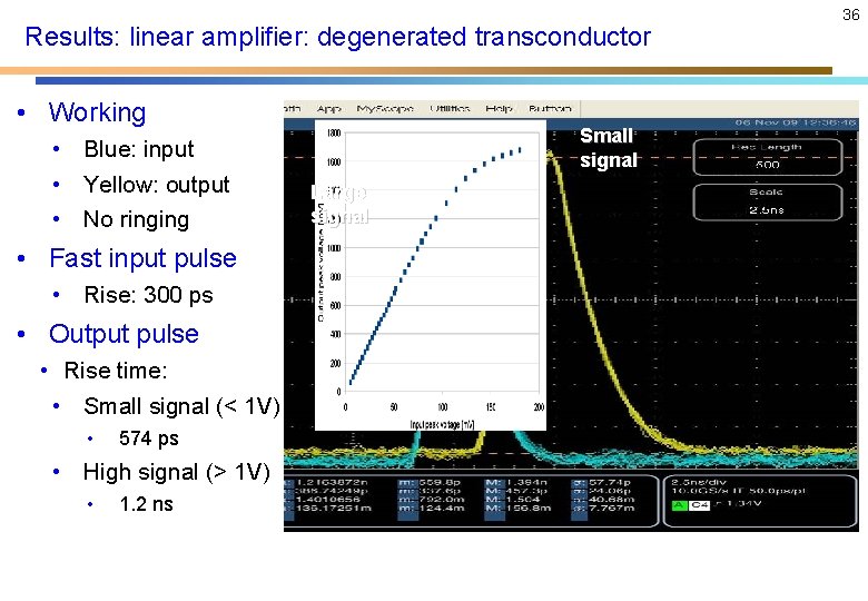
Results: linear amplifier: degenerated transconductor • Working • Blue: input • Yellow: output • No ringing • Fast input pulse • Rise: 300 ps • Output pulse • Rise time: • Small signal (< 1 V) • 574 ps • High signal (> 1 V) • 1. 2 ns Small signal Large signal 36
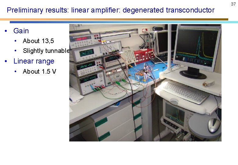
Preliminary results: linear amplifier: degenerated transconductor • Gain • About 13, 5 • Slightly tunnable • Linear range • About 1. 5 V 37
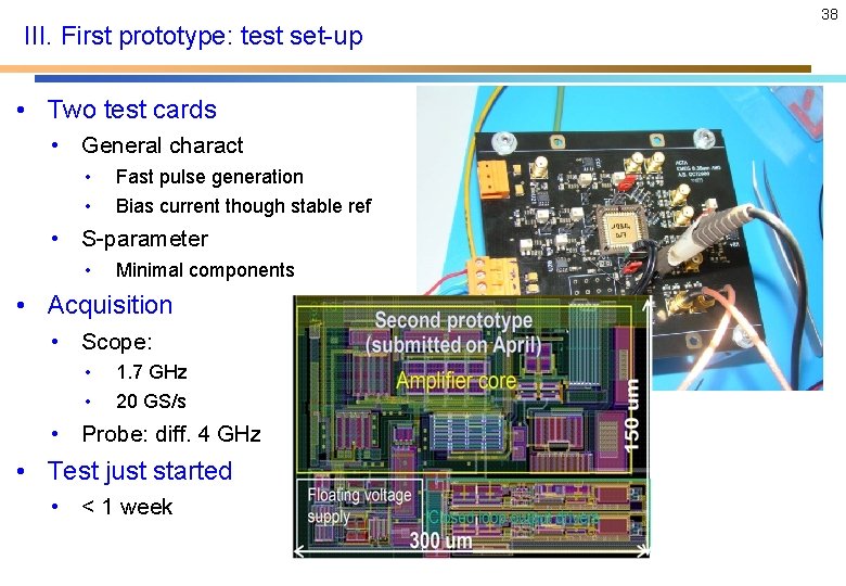
III. First prototype: test set-up • Two test cards • General charact • • Fast pulse generation Bias current though stable ref • S-parameter • Minimal components • Acquisition • Scope: • • 1. 7 GHz 20 GS/s • Probe: diff. 4 GHz • Test just started • < 1 week 38
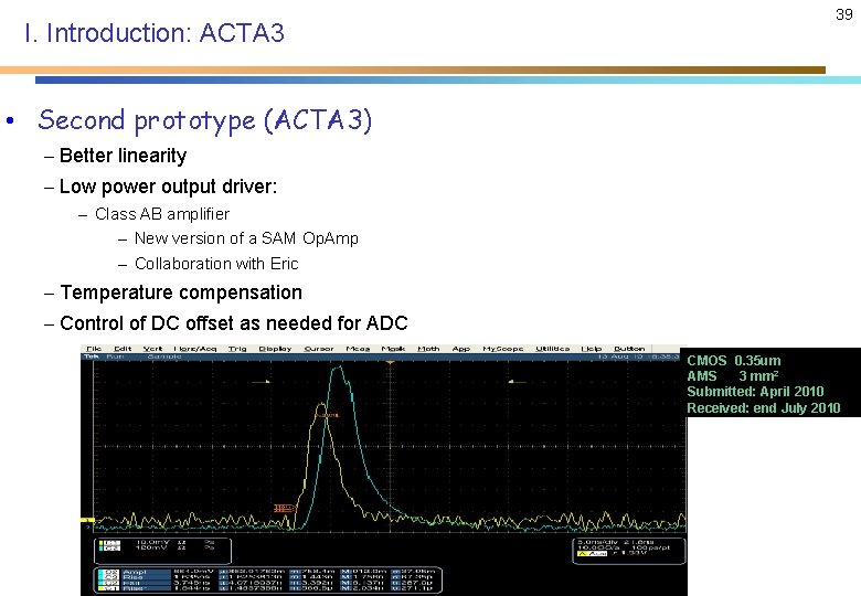
I. Introduction: ACTA 3 39 • Second prototype (ACTA 3) – Better linearity – Low power output driver: – Class AB amplifier – New version of a SAM Op. Amp – Collaboration with Eric – Temperature compensation – Control of DC offset as needed for ADC CMOS 0. 35 um AMS 3 mm 2 Submitted: April 2010 Received: end July 2010
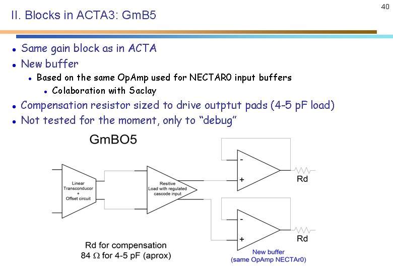
II. Blocks in ACTA 3: Gm. B 5 Same gain block as in ACTA New buffer Based on the same Op. Amp used for NECTAR 0 input buffers Colaboration with Saclay Compensation resistor sized to drive outptut pads (4 -5 p. F load) Not tested for the moment, only to “debug” 40
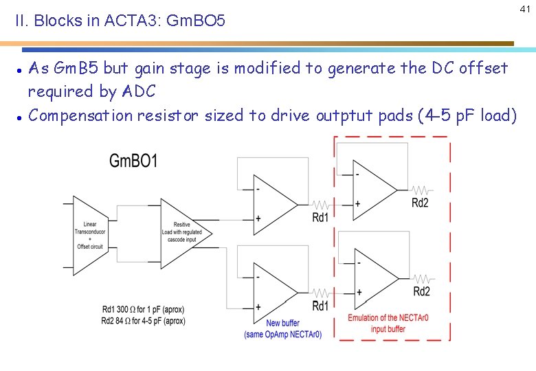
II. Blocks in ACTA 3: Gm. BO 5 As Gm. B 5 but gain stage is modified to generate the DC offset required by ADC Compensation resistor sized to drive outptut pads (4 -5 p. F load) 41
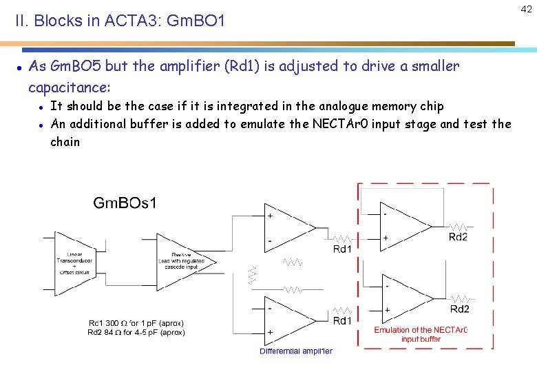
II. Blocks in ACTA 3: Gm. BO 1 As Gm. BO 5 but the amplifier (Rd 1) is adjusted to drive a smaller capacitance: It should be the case if it is integrated in the analogue memory chip An additional buffer is added to emulate the NECTAr 0 input stage and test the chain 42
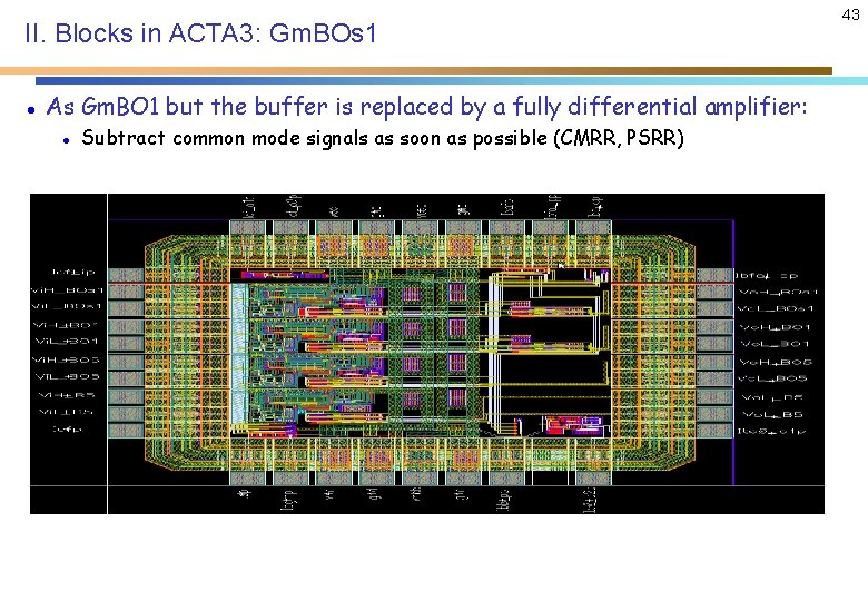
II. Blocks in ACTA 3: Gm. BOs 1 As Gm. BO 1 but the buffer is replaced by a fully differential amplifier: Subtract common mode signals as soon as possible (CMRR, PSRR) 43
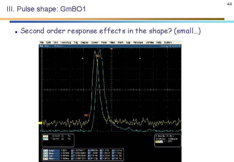
III. Pulse shape: Gm. BO 1 Second order response effects in the shape? (small…) 44
III. Pulse shape: Gm. BOs 1 Second order response effects in the shape? (small…) 45
III. Pulse shape: rise time vs amplitude 46
IV. Behaviour of the new buffer: class B boost control A current control Ibfol has to be set to > 30 u. A to be sure that the class B current boost is off at the quiescent state 47
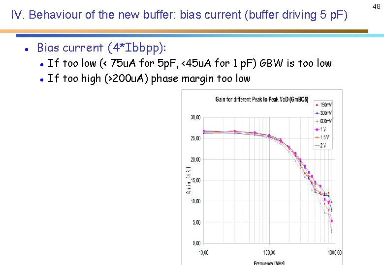
IV. Behaviour of the new buffer: bias current (buffer driving 5 p. F) Bias current (4*Ibbpp): If too low (< 75 u. A for 5 p. F, <45 u. A for 1 p. F) GBW is too low If too high (>200 u. A) phase margin too low 48
V. Bandwidth: Gm. BO 5 Nice first order response with little non-linearity up to 2 V, but… However BW is only 200 MHZ Rd was adjusted to have 300 MHz !!! With an external Cload of 3 p. F + extracted capacitances including pads 49
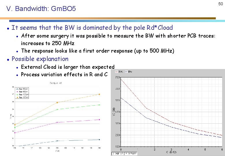
V. Bandwidth: Gm. BO 5 It seems that the BW is dominated by the pole Rd*Cload After some surgery it was possible to measure the BW with shorter PCB traces: increases to 250 MHz The response looks like a first order response (up to 500 MHz) Possible explanation External Cload is larger than expected Process variation effects in R and C 50
V. Bandwidth: Gm. BO 5 vs Gm. B 01 Additional confirmation that the BW is limited by the Rd*Cload The BW of Gm. BO 1 is even larger It has an additional buffer ! Should be possible to achieve > 300 MHz BW for the full amplification ACTA 3 + NECTAR 0 input buffer Need a very careful tuning of Rd Environment more controlled BW vs stability ACTA 3 in NECTAR silicon Postlayout simulation with Eric Side effect: Underestimation of lin error ? Seems to be enough margin… 51
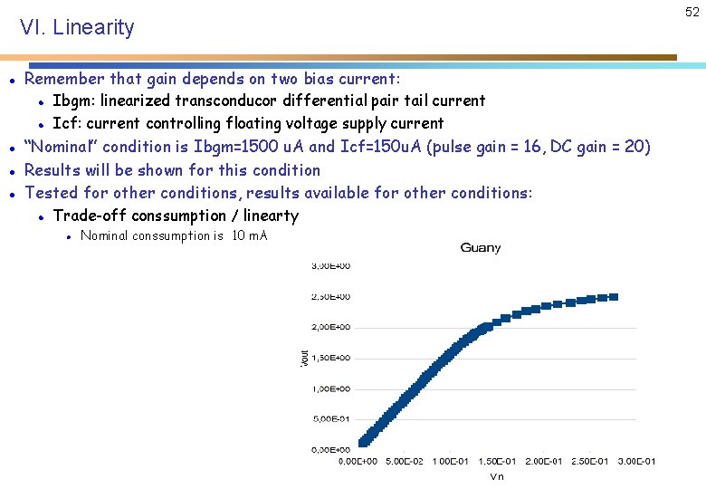
VI. Linearity Remember that gain depends on two bias current: Ibgm: linearized transconducor differential pair tail current Icf: current controlling floating voltage supply current “Nominal” condition is Ibgm=1500 u. A and Icf=150 u. A (pulse gain = 16, DC gain = 20) Results will be shown for this condition Tested for other conditions, results available for other conditions: Trade-off conssumption / linearty Nominal conssumption is 10 m. A 52
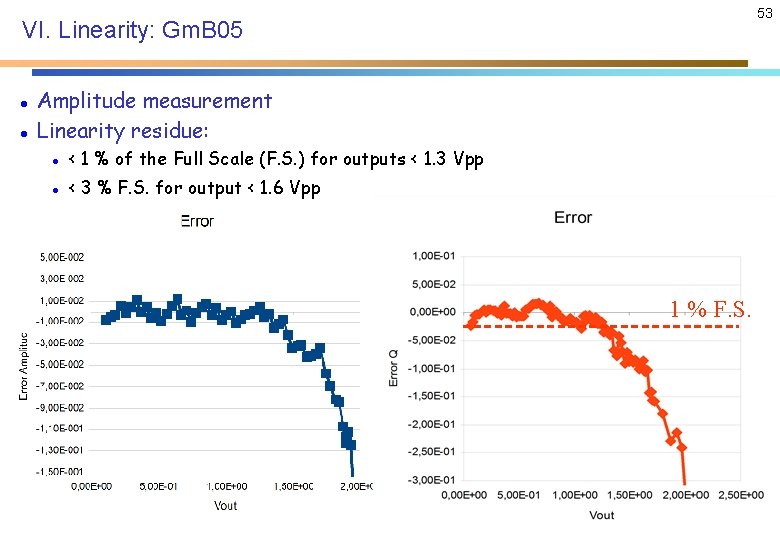
53 VI. Linearity: Gm. B 05 Amplitude measurement Linearity residue: < 1 % of the Full Scale (F. S. ) for outputs < 1. 3 Vpp < 3 % F. S. for output < 1. 6 Vpp 1 % F. S.
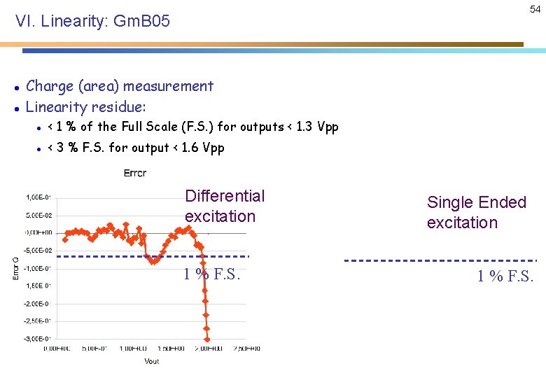
54 VI. Linearity: Gm. B 05 Charge (area) measurement Linearity residue: < 1 % of the Full Scale (F. S. ) for outputs < 1. 3 Vpp < 3 % F. S. for output < 1. 6 Vpp Differential excitation 1 % F. S. Single Ended excitation 1 % F. S.
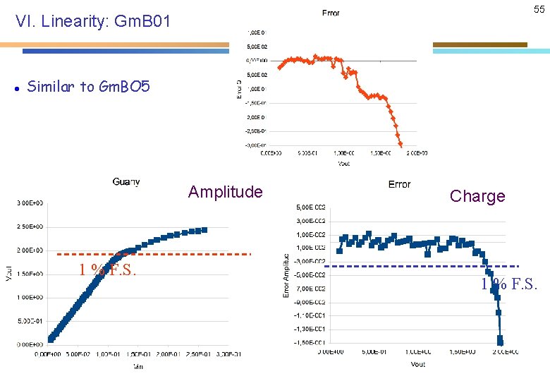
55 VI. Linearity: Gm. B 01 Similar to Gm. BO 5 Amplitude 1 % F. S. Charge 1 % F. S.
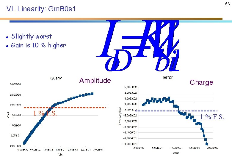
56 VI. Linearity: Gm. B 0 s 1 Slightly worst Gain is 10 % higher Amplitude 1 % F. S. Charge 1 % F. S.
IV. ACTA 3: Offset generation: effect on linearity and gain Linearity is ok at the gain plateau Optimal region around Ibof 300 u. A 57
- Slides: 57