1 Scratch Testing of Silicon Wafers for Surface
- Slides: 9

1 Scratch Testing of Silicon Wafers for Surface Characterization SFR Workshop November 8, 2000 Edward I. Hwang, David A. Dornfeld Berkeley, CA 2001 Goal: To build integrated CMP model for basic mechanical and chemical elements by 09/30/2001 11/8/2000

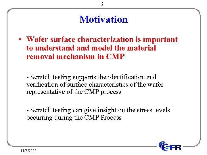
2 Motivation • Wafer surface characterization is important to understand model the material removal mechanism in CMP - Scratch testing supports the identification and verification of surface characteristics of the wafer representative of the CMP process - Scratch testing can give insight on the stress levels occurring during the CMP Process 11/8/2000

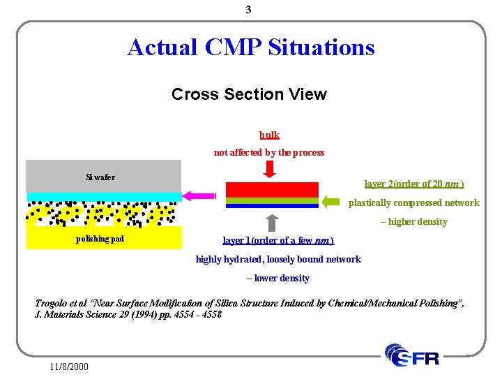
3 Actual CMP Situations Cross Section View bulk not affected by the process Si wafer layer 2(order of 20 nm ) plastically compressed network – higher density polishing pad layer 1(order of a few nm ) highly hydrated, loosely bound network – lower density Trogolo et al “Near Surface Modification of Silica Structure Induced by Chemical/Mechanical Polishing”, J. Materials Science 29 (1994) pp. 4554 - 4558 11/8/2000

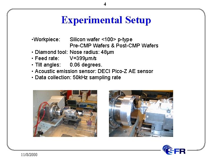
4 Experimental Setup • Workpiece: Silicon wafer <100> p-type Pre-CMP Wafers & Post-CMP Wafers • Diamond tool: Nose radius: 48μm • Feed rate: V=399μm/s • Tilt angles: 0. 06 degrees. • Acoustic emission sensor: DECI Pico-Z AE sensor • Data collection: 50 k. Hz sampling rate 11/8/2000

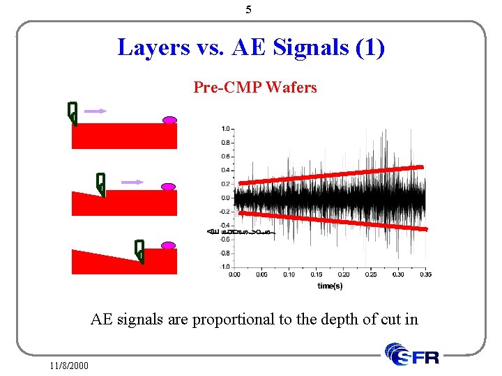
5 Layers vs. AE Signals (1) Pre-CMP Wafers AE signals are proportional to the depth of cut in 11/8/2000

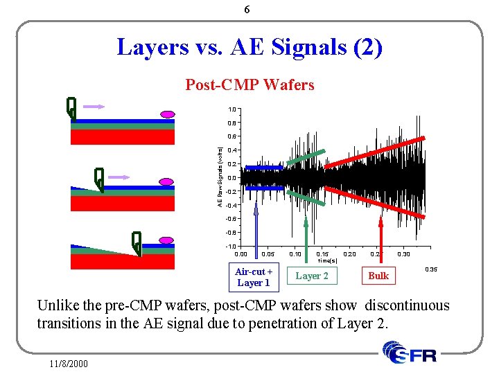
6 Layers vs. AE Signals (2) Post-CMP Wafers 1. 0 0. 8 AE Raw Signals (volts) 0. 6 0. 4 0. 2 0. 0 -0. 2 -0. 4 -0. 6 -0. 8 -1. 0 0. 05 0. 10 0. 15 0. 20 0. 25 0. 30 time(s) Air-cut + Layer 1 Layer 2 Bulk 0. 35 Unlike the pre-CMP wafers, post-CMP wafers show discontinuous transitions in the AE signal due to penetration of Layer 2. 11/8/2000

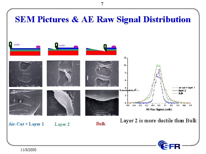
7 SEM Pictures & AE Raw Signal Distribution Air-Cut + Layer 1 11/8/2000 Layer 2 Bulk Layer 2 is more ductile than Bulk

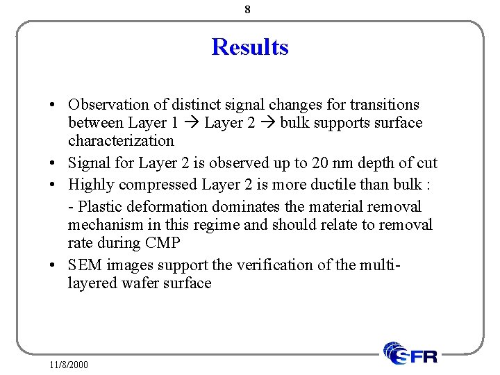
8 Results • Observation of distinct signal changes for transitions between Layer 1 Layer 2 bulk supports surface characterization • Signal for Layer 2 is observed up to 20 nm depth of cut • Highly compressed Layer 2 is more ductile than bulk : - Plastic deformation dominates the material removal mechanism in this regime and should relate to removal rate during CMP • SEM images support the verification of the multilayered wafer surface 11/8/2000

9 2002 & 2003 Goals Develop comprehensive chemical and mechanical model. Perform experimental and metrological validation, by 9/30/2003. • Replicate the scratch testing with AFM machine in order to be closer to actual CMP situations • Quantify the wafer surface characteristics in CMP 11/8/2000