1 Nanomaterials Synthesis 1 Prof P Ravindran Department
- Slides: 93

1 Nanomaterials Synthesis - 1 Prof. P. Ravindran, Department of Physics, Central University of Tamil Nadu, India & Center for Materials Science and Nanotechnology, University of Oslo, Norway http: //folk. uio. no/ravi/cutn/NMNT 2016 P. Ravindran, Nanomaterials and Nanotechnology, Spring 2016: Nanomaterials Synthesis - 1

Nano-size materials formation n n Growth from liquid phase, aqueous solutions Growth from gas phase, CVD, CVS Growth from vapor phase, PVD, MBE Sol-Gel solution, nano-particle formation Hydrogenation assisted growth P. Ravindran, Nanomaterials and Nanotechnology, Spring 2016: Nanomaterials Synthesis - 1

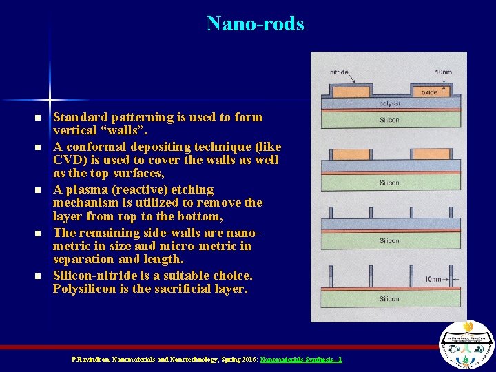
Nano-rods n n n Standard patterning is used to form vertical “walls”. A conformal depositing technique (like CVD) is used to cover the walls as well as the top surfaces, A plasma (reactive) etching mechanism is utilized to remove the layer from top to the bottom, The remaining side-walls are nanometric in size and micro-metric in separation and length. Silicon-nitride is a suitable choice. Polysilicon is the sacrificial layer. P. Ravindran, Nanomaterials and Nanotechnology, Spring 2016: Nanomaterials Synthesis - 1

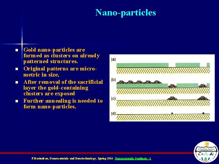
Nano-particles n n Gold nano-particles are formed as clusters on already patterned structures. Original patterns are micrometric in size, After removal of the sacrificial layer the gold-containing clusters are exposed Further annealing is needed to form nano-particles. P. Ravindran, Nanomaterials and Nanotechnology, Spring 2016: Nanomaterials Synthesis - 1

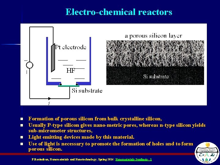
Electro-chemical reactors n n Formation of porous silicon from bulk crystalline silicon, Usually P-type silicon gives nano-metric pores, whereas n-type silicon yields sub-micrometer structures, Light emitting devices made by this material. Use of light is necessary to promote the formation of holes and to form porous silicon. P. Ravindran, Nanomaterials and Nanotechnology, Spring 2016: Nanomaterials Synthesis - 1

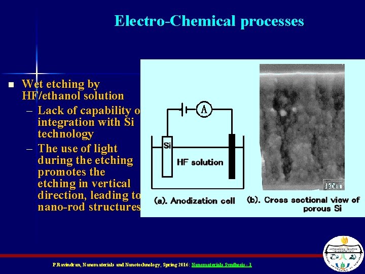
Electro-Chemical processes n Wet etching by HF/ethanol solution – Lack of capability of integration with Si technology – The use of light during the etching promotes the etching in vertical direction, leading to nano-rod structures. P. Ravindran, Nanomaterials and Nanotechnology, Spring 2016: Nanomaterials Synthesis - 1

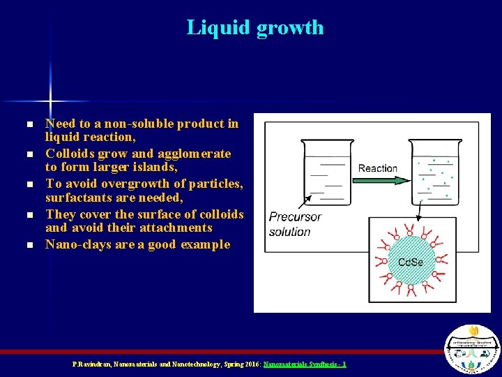
Liquid growth n n n Need to a non-soluble product in liquid reaction, Colloids grow and agglomerate to form larger islands, To avoid overgrowth of particles, surfactants are needed, They cover the surface of colloids and avoid their attachments Nano-clays are a good example P. Ravindran, Nanomaterials and Nanotechnology, Spring 2016: Nanomaterials Synthesis - 1

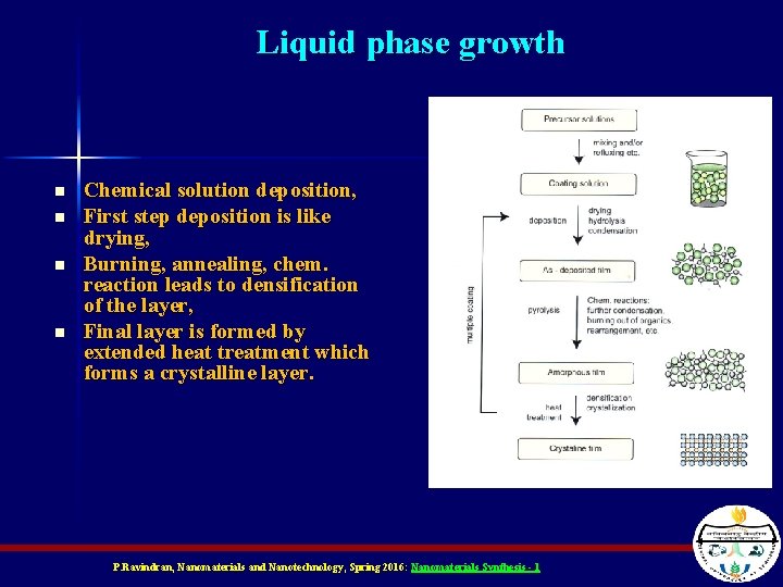
Liquid phase growth n n Chemical solution deposition, First step deposition is like drying, Burning, annealing, chem. reaction leads to densification of the layer, Final layer is formed by extended heat treatment which forms a crystalline layer. P. Ravindran, Nanomaterials and Nanotechnology, Spring 2016: Nanomaterials Synthesis - 1

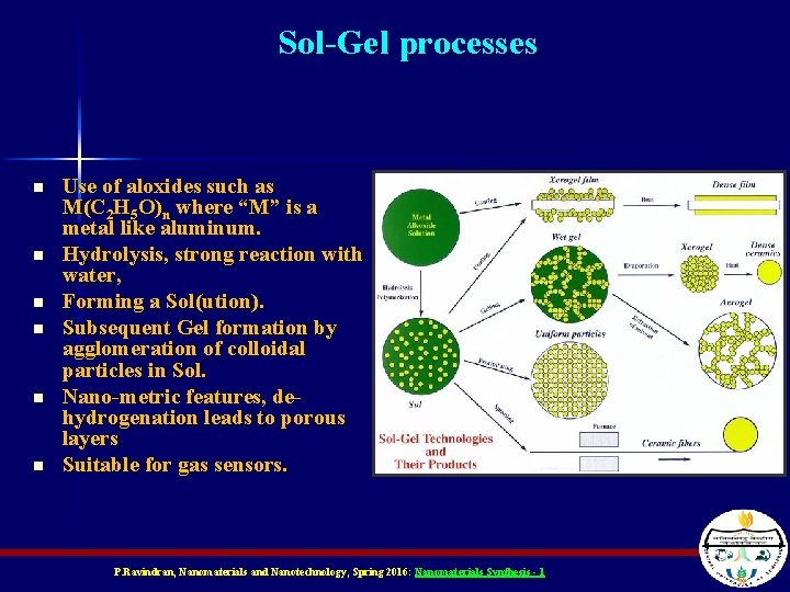
Sol-Gel processes n n n Use of aloxides such as M(C 2 H 5 O)n where “M” is a metal like aluminum. Hydrolysis, strong reaction with water, Forming a Sol(ution). Subsequent Gel formation by agglomeration of colloidal particles in Sol. Nano-metric features, dehydrogenation leads to porous layers Suitable for gas sensors. P. Ravindran, Nanomaterials and Nanotechnology, Spring 2016: Nanomaterials Synthesis - 1

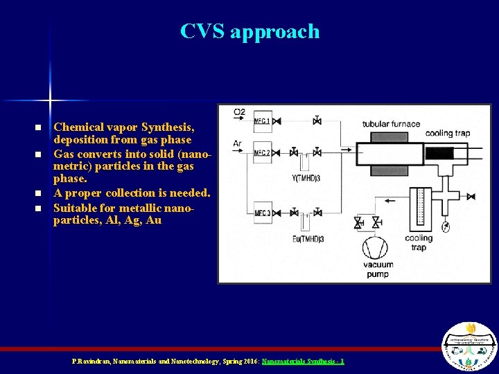
CVS approach n n Chemical vapor Synthesis, deposition from gas phase Gas converts into solid (nanometric) particles in the gas phase. A proper collection is needed. Suitable for metallic nanoparticles, Al, Ag, Au P. Ravindran, Nanomaterials and Nanotechnology, Spring 2016: Nanomaterials Synthesis - 1

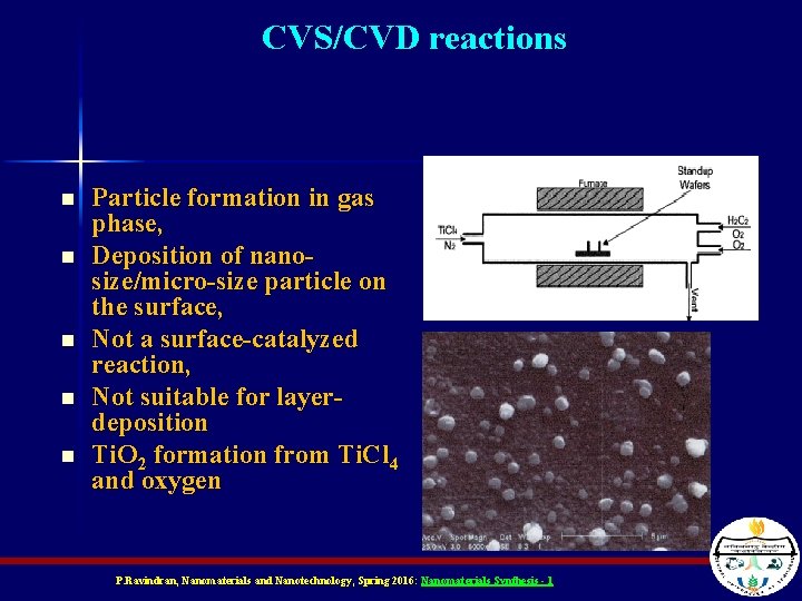
CVS/CVD reactions n n n Particle formation in gas phase, Deposition of nanosize/micro-size particle on the surface, Not a surface-catalyzed reaction, Not suitable for layerdeposition Ti. O 2 formation from Ti. Cl 4 and oxygen P. Ravindran, Nanomaterials and Nanotechnology, Spring 2016: Nanomaterials Synthesis - 1

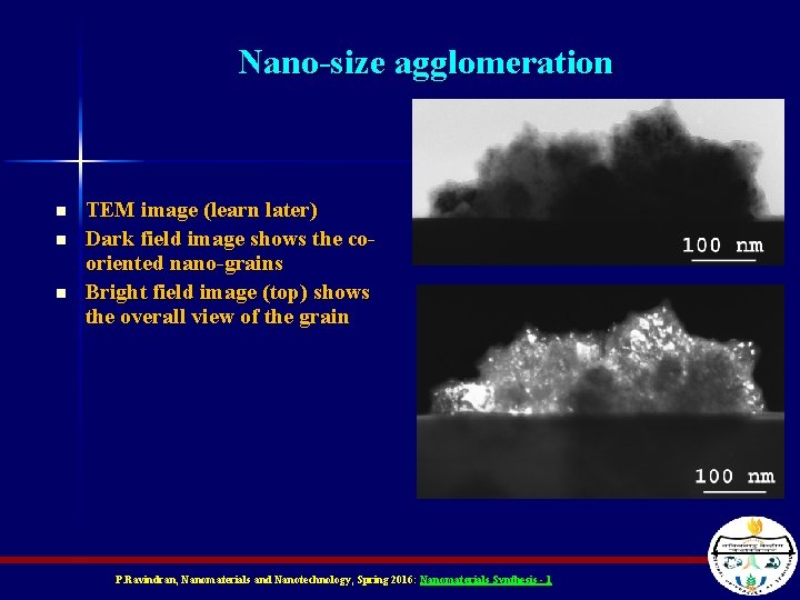
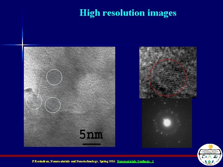
Nano-size agglomeration n TEM image (learn later) Dark field image shows the cooriented nano-grains Bright field image (top) shows the overall view of the grain P. Ravindran, Nanomaterials and Nanotechnology, Spring 2016: Nanomaterials Synthesis - 1

High resolution images P. Ravindran, Nanomaterials and Nanotechnology, Spring 2016: Nanomaterials Synthesis - 1

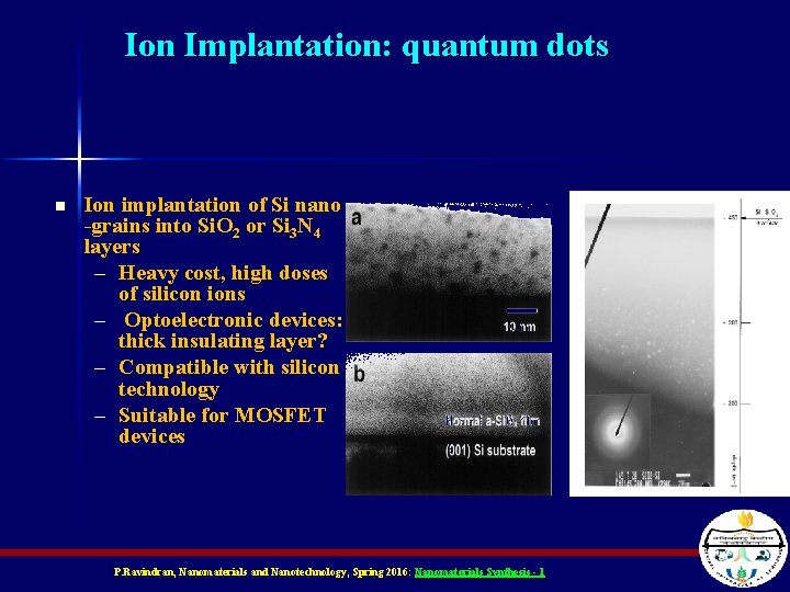
Ion Implantation: quantum dots n Ion implantation of Si nano -grains into Si. O 2 or Si 3 N 4 layers – Heavy cost, high doses of silicon ions – Optoelectronic devices: thick insulating layer? – Compatible with silicon technology – Suitable for MOSFET devices P. Ravindran, Nanomaterials and Nanotechnology, Spring 2016: Nanomaterials Synthesis - 1

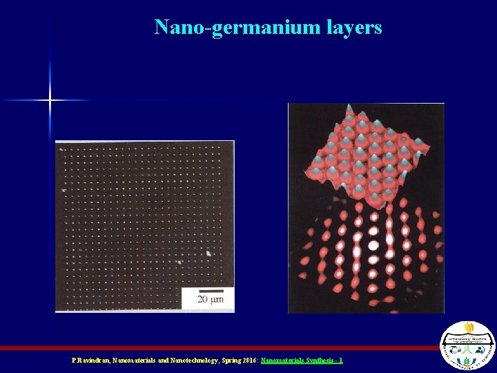
Nano-germanium layers P. Ravindran, Nanomaterials and Nanotechnology, Spring 2016: Nanomaterials Synthesis - 1

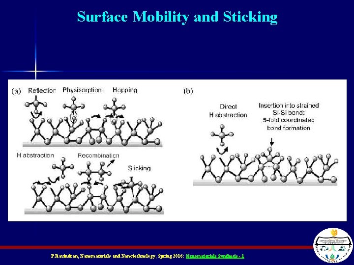
Deposition: Physical Methods n n Physical deposition means that nm sized chunks of material fly at the substrate and stick onto it The hotter the substrate, the more easily these pieces of material can move around (surface mobility) – They find their point of lowest energy resulting in a better film P. Ravindran, Nanomaterials and Nanotechnology, Spring 2016: Nanomaterials Synthesis - 1

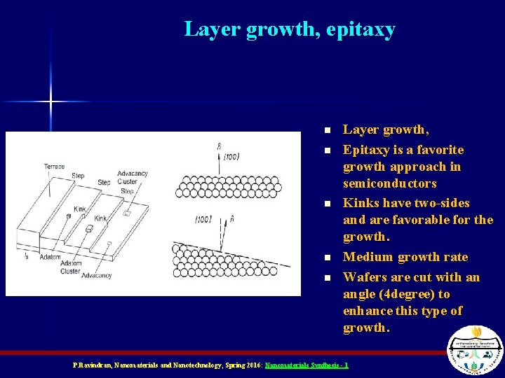
Layer growth, epitaxy n n n Layer growth, Epitaxy is a favorite growth approach in semiconductors Kinks have two-sides and are favorable for the growth. Medium growth rate Wafers are cut with an angle (4 degree) to enhance this type of growth. P. Ravindran, Nanomaterials and Nanotechnology, Spring 2016: Nanomaterials Synthesis - 1

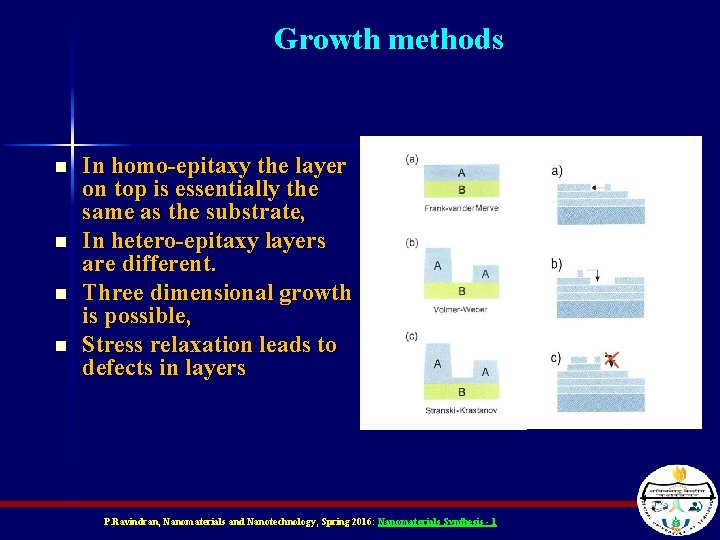
Growth methods n n In homo-epitaxy the layer on top is essentially the same as the substrate, In hetero-epitaxy layers are different. Three dimensional growth is possible, Stress relaxation leads to defects in layers P. Ravindran, Nanomaterials and Nanotechnology, Spring 2016: Nanomaterials Synthesis - 1

Growth vs. Nucleation n n n n There are two stages of the film formation: the initial formation of the little islands or Nucleation and the aggregation of such islands to form a continuous layer (growth). dni/dt= (Rads + Rdet + 2 R 1) – (Revap + Rcap +2 R’ 1) n 1: concentration of individual adatoms, n 2: pairs of adatoms, n 3: clusters of size three, … Rads: rate of adsorption of individual adatoms, Rdet: detachment of atoms from larger clusters, Revap: rate of evaporation, Rcap: rate of capture by larger clusters, R 1 : rate of breaking of pairs and R’ 1: rate of formation of pairs. dn 2/dt: rate of changing the pairs, dn 3/dt: triplet atoms , … P. Ravindran, Nanomaterials and Nanotechnology, Spring 2016: Nanomaterials Synthesis - 1

Growth vs. Nucleation n n n At the second stage, that is the aggregation of small islands, the Gibbs free energy rules. We have three cases, the energy of the free-surface (Gsur-vac), energy of the covered surface with the layer (Gsur-lay) and the energy stored in the layer with respect to vacuum (Glay-vac). G=Gsur-vac (1 -ε) + (Gsur-lay + Glay-vac) ε Here “ε” is the percentage of coverage. If Gsur-vac > (Gsur-lay + Glay-vac) increase in “fraction” leads to a reduction in the overall energy, so it is favorable (Frank-vander-Merve mode) If Gsur-vac < (Gsur-lay + Glay-vac) increase in “fraction” results in an increment in the overall energy, not favorable (Volmer-Weber growth). P. Ravindran, Nanomaterials and Nanotechnology, Spring 2016: Nanomaterials Synthesis - 1

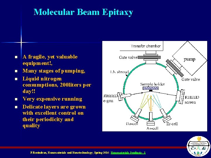
Molecular Beam Epitaxy n n n A fragile, yet valuable equipment!, Many stages of pumping, Liquid nitrogen consumptions, 200 liters per day!! Very expensive running Delicate layers are grown with excellent control on their periodicity and quality P. Ravindran, Nanomaterials and Nanotechnology, Spring 2016: Nanomaterials Synthesis - 1

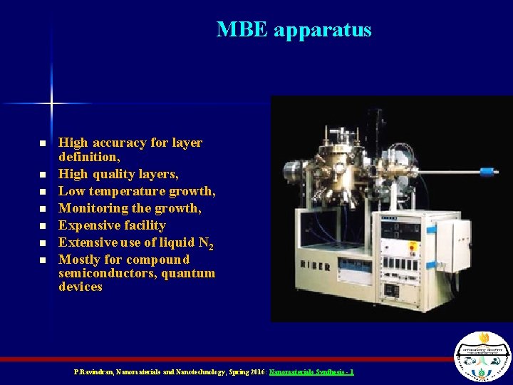
MBE apparatus n n n n High accuracy for layer definition, High quality layers, Low temperature growth, Monitoring the growth, Expensive facility Extensive use of liquid N 2 Mostly for compound semiconductors, quantum devices P. Ravindran, Nanomaterials and Nanotechnology, Spring 2016: Nanomaterials Synthesis - 1

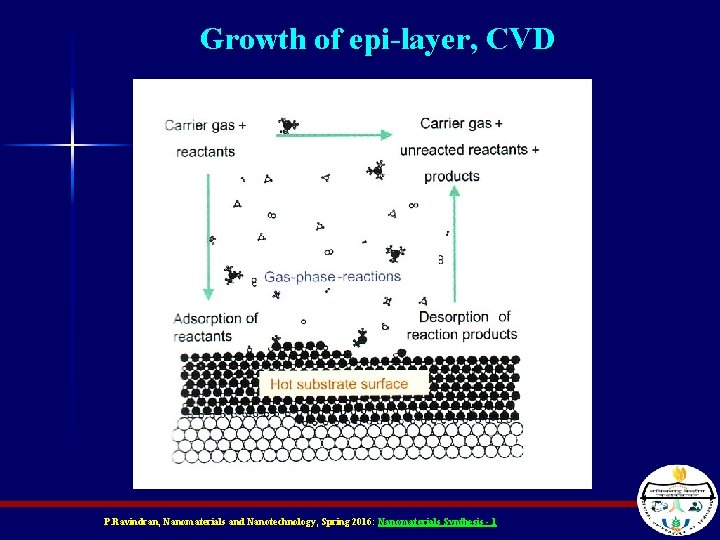
Growth of epi-layer, CVD P. Ravindran, Nanomaterials and Nanotechnology, Spring 2016: Nanomaterials Synthesis - 1

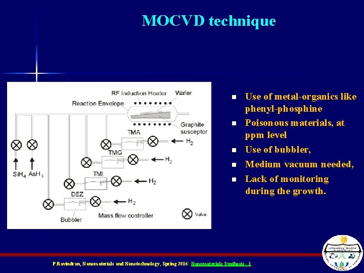
MOCVD technique n n n Use of metal-organics like phenyl-phosphine Poisonous materials, at ppm level Use of bubbler, Medium vacuum needed, Lack of monitoring during the growth. P. Ravindran, Nanomaterials and Nanotechnology, Spring 2016: Nanomaterials Synthesis - 1

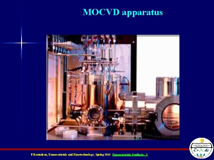
MOCVD apparatus P. Ravindran, Nanomaterials and Nanotechnology, Spring 2016: Nanomaterials Synthesis - 1

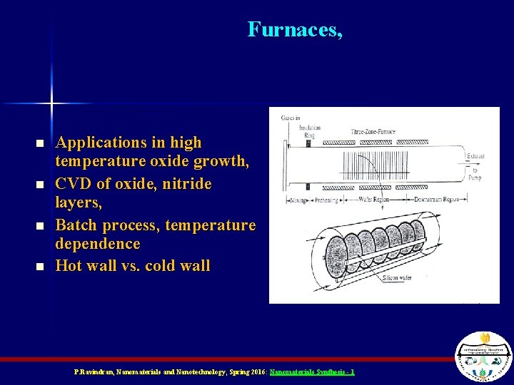
Furnaces, n n Applications in high temperature oxide growth, CVD of oxide, nitride layers, Batch process, temperature dependence Hot wall vs. cold wall P. Ravindran, Nanomaterials and Nanotechnology, Spring 2016: Nanomaterials Synthesis - 1

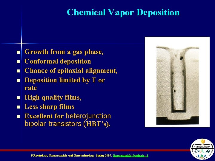
Chemical Vapor Deposition n n n Growth from a gas phase, Conformal deposition Chance of epitaxial alignment, Deposition limited by T or rate High quality films, Less sharp films Excellent for heterojunction bipolar transistors (HBT’s). P. Ravindran, Nanomaterials and Nanotechnology, Spring 2016: Nanomaterials Synthesis - 1

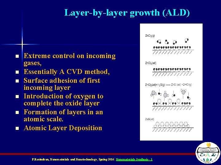
Layer-by-layer growth (ALD) n n n Extreme control on incoming gases, Essentially A CVD method, Surface adhesion of first incoming layer Introduction of oxygen to complete the oxide layer Formation of layers in an atomic scale. Atomic Layer Deposition P. Ravindran, Nanomaterials and Nanotechnology, Spring 2016: Nanomaterials Synthesis - 1

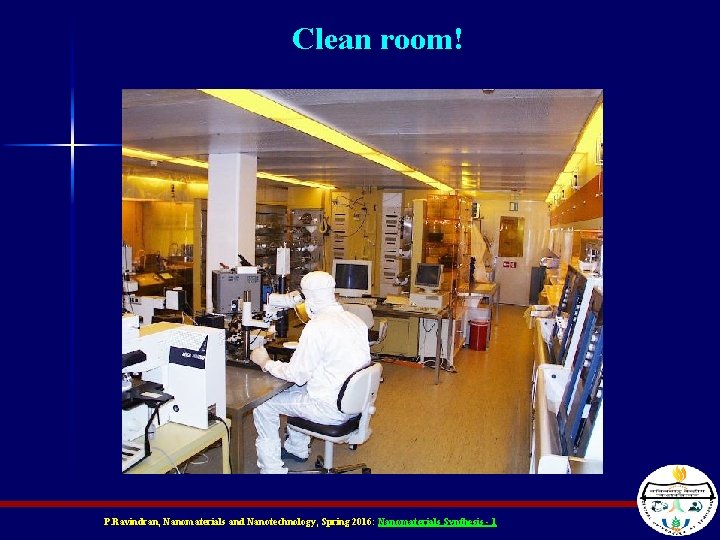
Clean room! P. Ravindran, Nanomaterials and Nanotechnology, Spring 2016: Nanomaterials Synthesis - 1

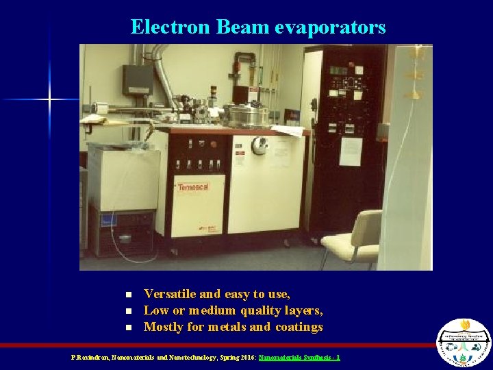
Electron Beam evaporators n n n Versatile and easy to use, Low or medium quality layers, Mostly for metals and coatings P. Ravindran, Nanomaterials and Nanotechnology, Spring 2016: Nanomaterials Synthesis - 1

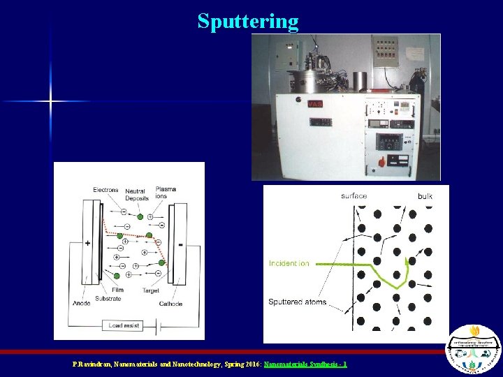
Sputtering P. Ravindran, Nanomaterials and Nanotechnology, Spring 2016: Nanomaterials Synthesis - 1

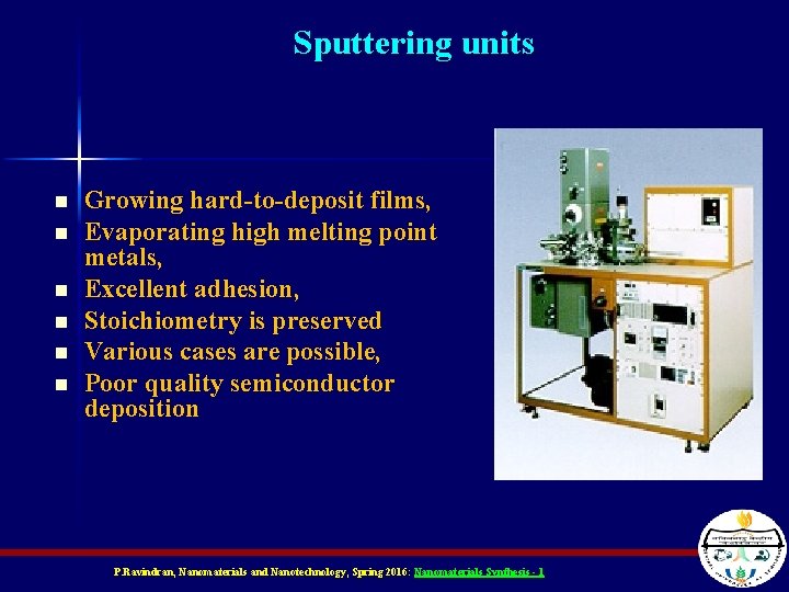
Sputtering units n n n Growing hard-to-deposit films, Evaporating high melting point metals, Excellent adhesion, Stoichiometry is preserved Various cases are possible, Poor quality semiconductor deposition P. Ravindran, Nanomaterials and Nanotechnology, Spring 2016: Nanomaterials Synthesis - 1

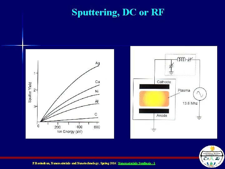
Sputtering, DC or RF P. Ravindran, Nanomaterials and Nanotechnology, Spring 2016: Nanomaterials Synthesis - 1

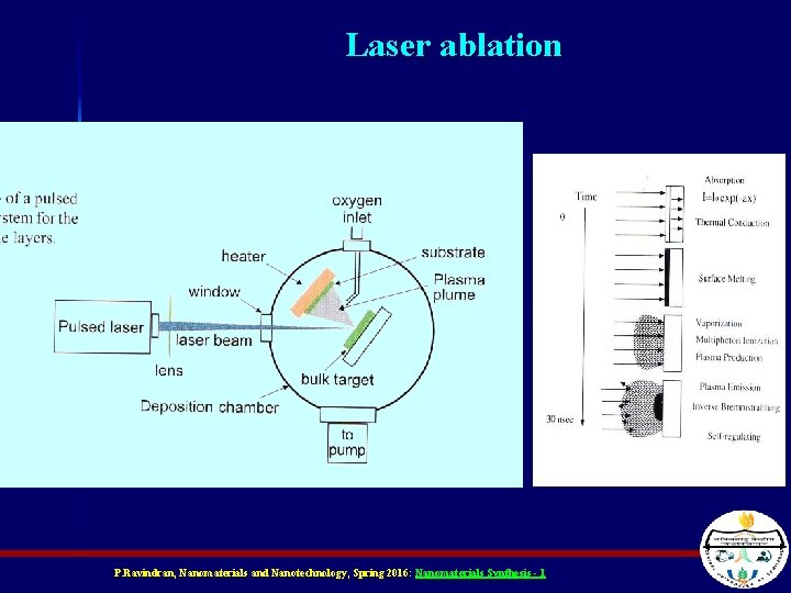
Laser ablation P. Ravindran, Nanomaterials and Nanotechnology, Spring 2016: Nanomaterials Synthesis - 1

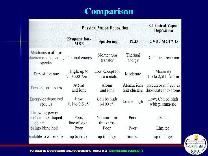
Comparison P. Ravindran, Nanomaterials and Nanotechnology, Spring 2016: Nanomaterials Synthesis - 1

Surface Mobility and Sticking P. Ravindran, Nanomaterials and Nanotechnology, Spring 2016: Nanomaterials Synthesis - 1

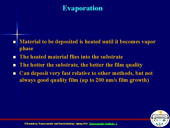
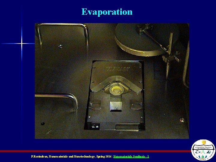
Evaporation n n Material to be deposited is heated until it becomes vapor phase The heated material flies into the substrate The hotter the substrate, the better the film quality Can deposit very fast relative to other methods, but not always good quality film (up to 200 nm/s film growth) P. Ravindran, Nanomaterials and Nanotechnology, Spring 2016: Nanomaterials Synthesis - 1

Evaporation P. Ravindran, Nanomaterials and Nanotechnology, Spring 2016: Nanomaterials Synthesis - 1

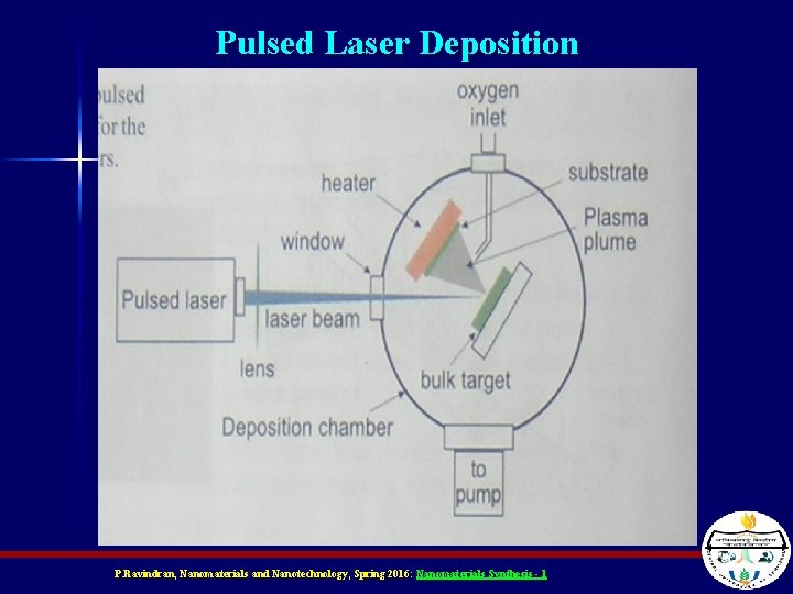
Pulsed Laser Deposition n Similar to Evaporation method, except uses a laser to heat the material to be deposited Different because the intense energy creates a plasma Plasmas not only contain inert material, but also ions and radicals which could chemically react with the surface – Depends on chemistry of reactants P. Ravindran, Nanomaterials and Nanotechnology, Spring 2016: Nanomaterials Synthesis - 1

Pulsed Laser Deposition P. Ravindran, Nanomaterials and Nanotechnology, Spring 2016: Nanomaterials Synthesis - 1

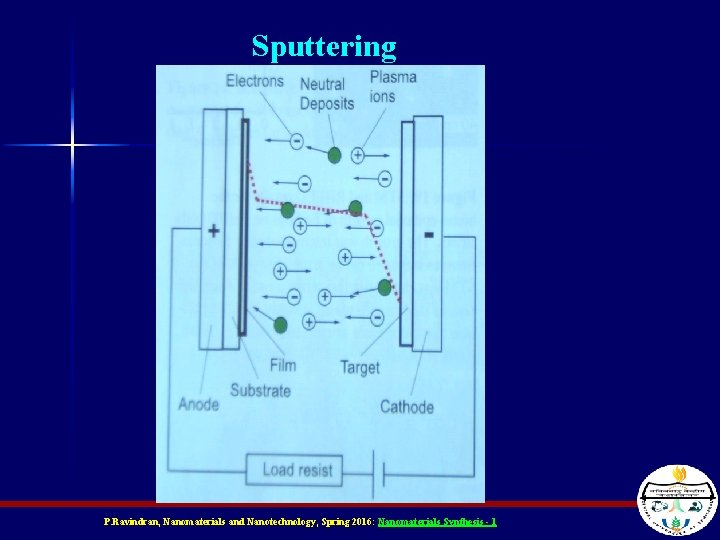
Sputtering n n The target (material to be deposited) and substrate are placed facing each other A plasma is ignited between them under vacuum A voltage bias between them causes ions from the plasma to ram into the target The ions eject pieces of the target that “sputter” onto the substrate P. Ravindran, Nanomaterials and Nanotechnology, Spring 2016: Nanomaterials Synthesis - 1

Sputtering P. Ravindran, Nanomaterials and Nanotechnology, Spring 2016: Nanomaterials Synthesis - 1

Magnetron Sputtering n n A big magnet is used to force the electrons into spiral paths so that they spend more time ionizing neutral gas particles This increases the number of ions More ions increases the chances of knocking out some of the material to be sputtered Increases efficiency P. Ravindran, Nanomaterials and Nanotechnology, Spring 2016: Nanomaterials Synthesis - 1

Deposition: Chemical Methods n n In chemical deposition, the material being deposited on the substrate reacts with the surface – Form bonds with the surface – Chemical reaction with the surface The substrate as well as reactant temperature play a role in the rate of reaction P. Ravindran, Nanomaterials and Nanotechnology, Spring 2016: Nanomaterials Synthesis - 1

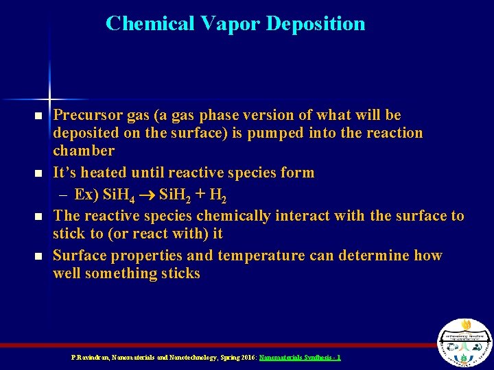
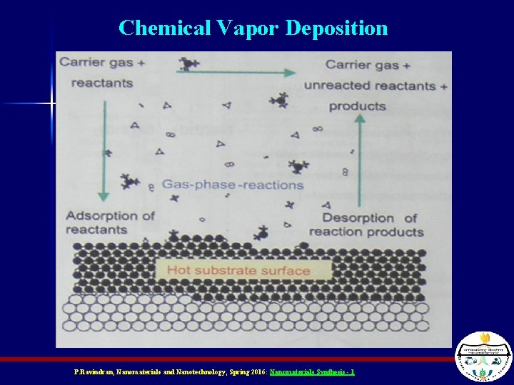
Chemical Vapor Deposition n n Precursor gas (a gas phase version of what will be deposited on the surface) is pumped into the reaction chamber It’s heated until reactive species form – Ex) Si. H 4 Si. H 2 + H 2 The reactive species chemically interact with the surface to stick to (or react with) it Surface properties and temperature can determine how well something sticks P. Ravindran, Nanomaterials and Nanotechnology, Spring 2016: Nanomaterials Synthesis - 1

Chemical Vapor Deposition P. Ravindran, Nanomaterials and Nanotechnology, Spring 2016: Nanomaterials Synthesis - 1

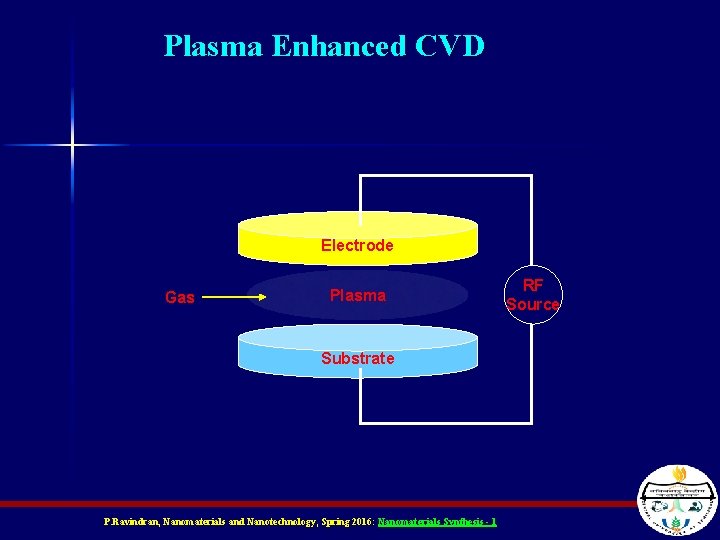
Plasma Enhanced CVD n n Uses an RF or microwave E-field to strip electrons off the precursor gasses Since e- are so much lighter than the rest of the molecule (ion), they accelerate in the E-field faster than the molecules P. Ravindran, Nanomaterials and Nanotechnology, Spring 2016: Nanomaterials Synthesis - 1

Plasma Enhanced CVD n n n By the time the E-field changes direction (at RF or microwave frequencies) the electron has gained a lot of momentum and the remaining molecule (ion) has barely started to move Thus, the e- have a high temperature and the molecules (ions) have a low temperature This means that the substrate can have a lower temperature, too – Enables new substrates like glass and plastic – This is how TFT-LCD displays can be made P. Ravindran, Nanomaterials and Nanotechnology, Spring 2016: Nanomaterials Synthesis - 1

Plasma Enhanced CVD Electrode Gas Plasma Substrate P. Ravindran, Nanomaterials and Nanotechnology, Spring 2016: Nanomaterials Synthesis - 1 RF Source

Optical CVD n n n Not always applicable Uses different wavelengths of light to break precursor gas bond to form reactive species – Ex) Cl 2 + h (photon) 2 Cl (radicals) Also enables low temperature deposition P. Ravindran, Nanomaterials and Nanotechnology, Spring 2016: Nanomaterials Synthesis - 1

Chemical Solution Deposition n Material is deposited on the substrate in the liquid state – Spin Coating: Some liquid is placed on the substrate and it’s spun really fast until only a thin coating is left – Dip Coating: Dunk the substrate in solution – Spray Coating: Like spray painting the substrate – Screen Printing: Put a stencil on the substrate and use a squeegee to pull solution across – Ink-jet Printing: Same as in an ink-jet printer for a PC P. Ravindran, Nanomaterials and Nanotechnology, Spring 2016: Nanomaterials Synthesis - 1

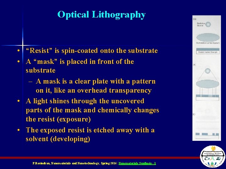
Lithography n n When a pattern is applied to the substrate The most common is optical lithography where a mask is used to expose a pattern onto a substrate – Like how a transparency on an overhead projector works The better the lithography, the smaller the feature size Small feature size nanoelectronics P. Ravindran, Nanomaterials and Nanotechnology, Spring 2016: Nanomaterials Synthesis - 1

Optical Lithography • “Resist” is spin-coated onto the substrate • A “mask” is placed in front of the substrate – A mask is a clear plate with a pattern on it, like an overhead transparency • A light shines through the uncovered parts of the mask and chemically changes the resist (exposure) • The exposed resist is etched away with a solvent (developing) P. Ravindran, Nanomaterials and Nanotechnology, Spring 2016: Nanomaterials Synthesis - 1

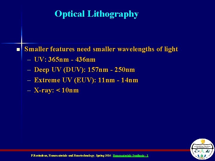
Optical Lithography n Smaller features need smaller wavelengths of light – UV: 365 nm - 436 nm – Deep UV (DUV): 157 nm - 250 nm – Extreme UV (EUV): 11 nm - 14 nm – X-ray: < 10 nm P. Ravindran, Nanomaterials and Nanotechnology, Spring 2016: Nanomaterials Synthesis - 1

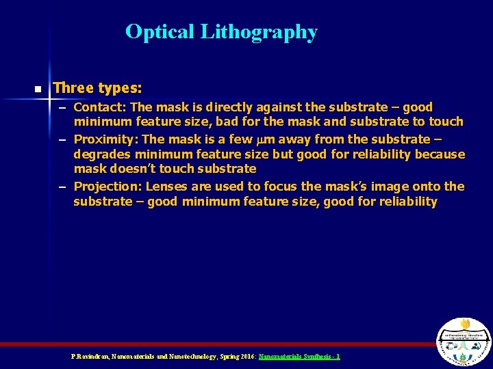
Optical Lithography n Three types: – Contact: The mask is directly against the substrate – good minimum feature size, bad for the mask and substrate to touch – Proximity: The mask is a few m away from the substrate – degrades minimum feature size but good for reliability because mask doesn’t touch substrate – Projection: Lenses are used to focus the mask’s image onto the substrate – good minimum feature size, good for reliability P. Ravindran, Nanomaterials and Nanotechnology, Spring 2016: Nanomaterials Synthesis - 1

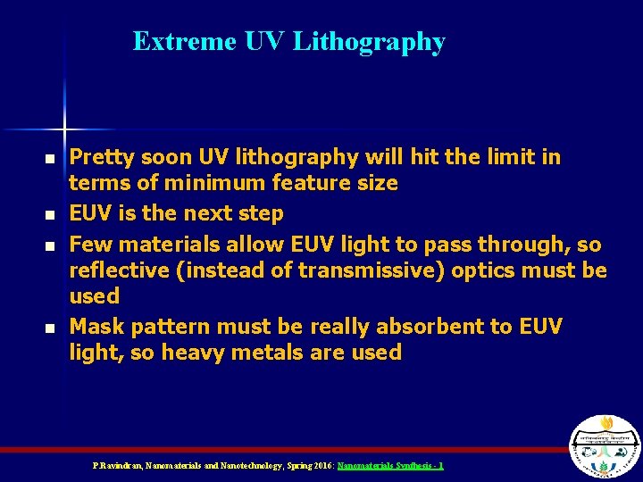
Extreme UV Lithography n n Pretty soon UV lithography will hit the limit in terms of minimum feature size EUV is the next step Few materials allow EUV light to pass through, so reflective (instead of transmissive) optics must be used Mask pattern must be really absorbent to EUV light, so heavy metals are used P. Ravindran, Nanomaterials and Nanotechnology, Spring 2016: Nanomaterials Synthesis - 1

X-ray Lithography n n n After EUV comes X-ray lithography Enables super-high resolution pattern transfer There are technical hurdles to overcome before x-ray lithography systems are in place – Synchrotrons need to be further developed as a source for x-rays P. Ravindran, Nanomaterials and Nanotechnology, Spring 2016: Nanomaterials Synthesis - 1

E-beam Lithography n n n Uses a focused beam of electrons to directly write to the substrate Works much like a CRT TV – an electron gun fires electrons and the beam is directed with magnetic fields There is a limit to how many electrons can be in the beam because they will start to repel each other and blur the beam P. Ravindran, Nanomaterials and Nanotechnology, Spring 2016: Nanomaterials Synthesis - 1

E-beam Lithography n n n Very precise, but very slow method Can be accomplished in two ways: – Use a narrow beam and turn it on and off to write or not write a pixel – Use a wide beam and a mask to block the parts that shouldn’t be written Typically very slow and costly – good for making optical lithographic masks for use in UV, EUV, and X-ray P. Ravindran, Nanomaterials and Nanotechnology, Spring 2016: Nanomaterials Synthesis - 1

Nano-imprint Technology n n Much like forging steel, except at a very small scale A stamp is fabricated at the nm-scale using traditional process methods A substrate is coated with some kind of polymer The polymer is stamped with the nm-scale stamp – The polymer is either cured with heat or light P. Ravindran, Nanomaterials and Nanotechnology, Spring 2016: Nanomaterials Synthesis - 1

Layer by Layer (LBL) Assembly n It was first reported by Iler in 1966 that multilayer thin film can be fabricated by alternative deposition of oppositely charged nanoparticles. n In addition to charged colloids, they also pointed out the potentials of using other charged species such as polyvalent ions, surfactants, water soluble polymer and even proteins to build the multilayer assembly. P. Ravindran, Nanomaterials and Nanotechnology, Spring 2016: Nanomaterials Synthesis - 1

LBL Assembly Awareness n Ø Iler’s suggestive work did not get public attention until later. Decher and Hong rediscovered and established the work in this area. In 1997, a feature article named “Fuzzy Nanoassemblies: Toward Layered Polymeric Multicomposites”, published in Science by Decher, systematically reviewed the work of LBL assembly. P. Ravindran, Nanomaterials and Nanotechnology, Spring 2016: Nanomaterials Synthesis - 1

Basis of LBL Assembly n LBL assembly can be built through conventional methods such as: velectrostatic interactions vhydrogen bonding vstep by step reaction vmolecular recognition and biorecognition P. Ravindran, Nanomaterials and Nanotechnology, Spring 2016: Nanomaterials Synthesis - 1

LBL Assembly Technique n The preparation of LBL is relatively easy without sophisticated procedures or instruments. Beakers containing dipping solutions and waters are all we need. n Substrates with cleaned hydrophilic surfaces such as glass, silica or mica, which exhibit a nonzero surface charge, must be employed. P. Ravindran, Nanomaterials and Nanotechnology, Spring 2016: Nanomaterials Synthesis - 1

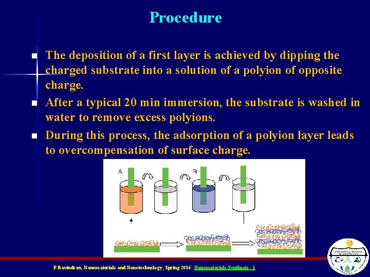
Procedure n n n The deposition of a first layer is achieved by dipping the charged substrate into a solution of a polyion of opposite charge. After a typical 20 min immersion, the substrate is washed in water to remove excess polyions. During this process, the adsorption of a polyion layer leads to overcompensation of surface charge. P. Ravindran, Nanomaterials and Nanotechnology, Spring 2016: Nanomaterials Synthesis - 1

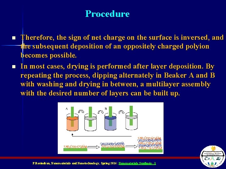
Procedure n n Therefore, the sign of net charge on the surface is inversed, and the subsequent deposition of an oppositely charged polyion becomes possible. In most cases, drying is performed after layer deposition. By repeating the process, dipping alternately in Beaker A and B with washing and drying in between, a multilayer assembly with the desired number of layers can be built up. P. Ravindran, Nanomaterials and Nanotechnology, Spring 2016: Nanomaterials Synthesis - 1

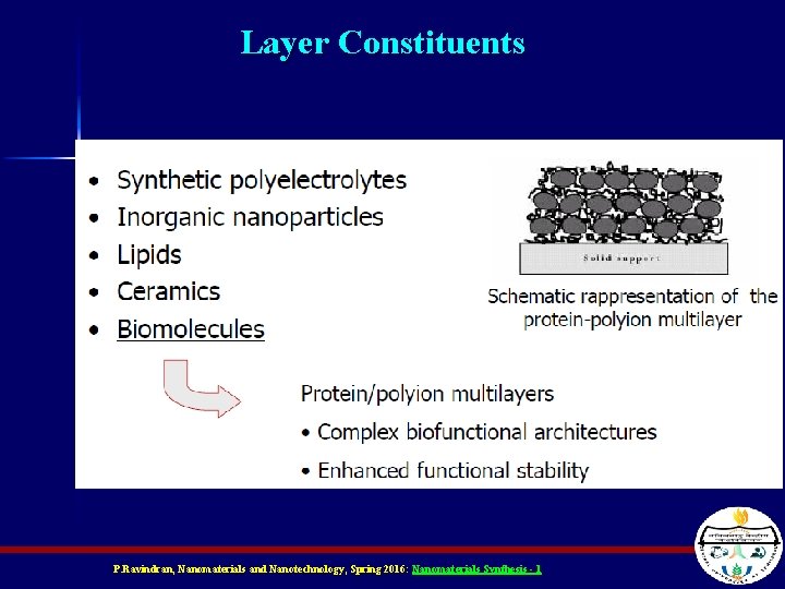
Layer Constituents P. Ravindran, Nanomaterials and Nanotechnology, Spring 2016: Nanomaterials Synthesis - 1

Advantages n There are many advantages using LBL assembly over other strategies for ultrathin film preparation such as the Langmuir-Blodgett (LB) technique and the self-assembled monolayer (SAM) method. P. Ravindran, Nanomaterials and Nanotechnology, Spring 2016: Nanomaterials Synthesis - 1

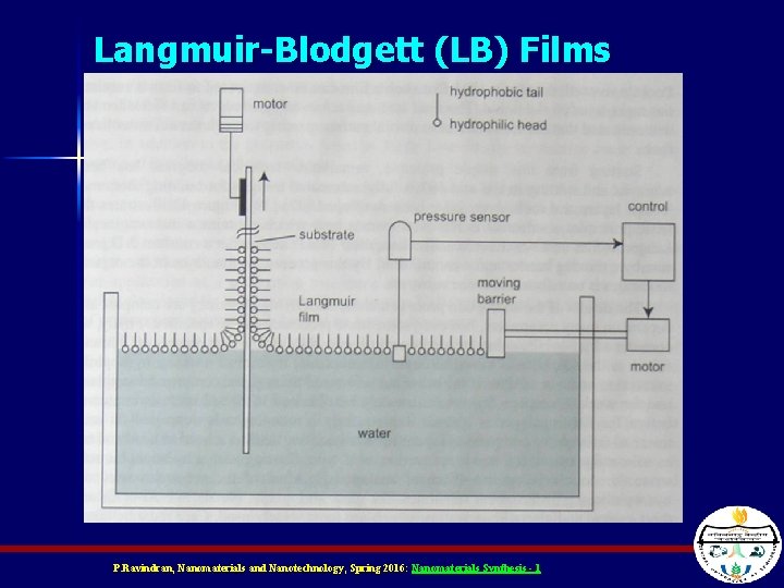
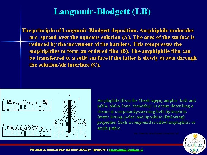
Langmuir-Blodgett (LB) Films n n A form of dip coating You have a solution with a layer of special molecules on the surface One side of the molecule is water-soluble, and the other is not (like soap) Thus all the molecules are aligned on top of the solution P. Ravindran, Nanomaterials and Nanotechnology, Spring 2016: Nanomaterials Synthesis - 1

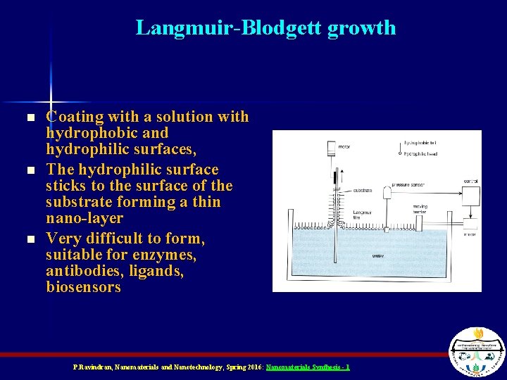
Langmuir-Blodgett growth n n n Coating with a solution with hydrophobic and hydrophilic surfaces, The hydrophilic surface sticks to the surface of the substrate forming a thin nano-layer Very difficult to form, suitable for enzymes, antibodies, ligands, biosensors P. Ravindran, Nanomaterials and Nanotechnology, Spring 2016: Nanomaterials Synthesis - 1

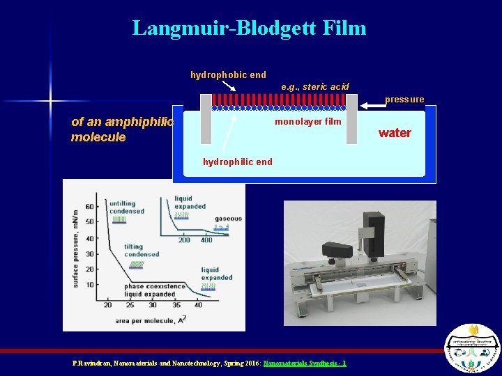
Langmuir-Blodgett Film hydrophobic end e. g. , steric acid pressure of an amphiphilic molecule monolayer film hydrophilic end P. Ravindran, Nanomaterials and Nanotechnology, Spring 2016: Nanomaterials Synthesis - 1 water

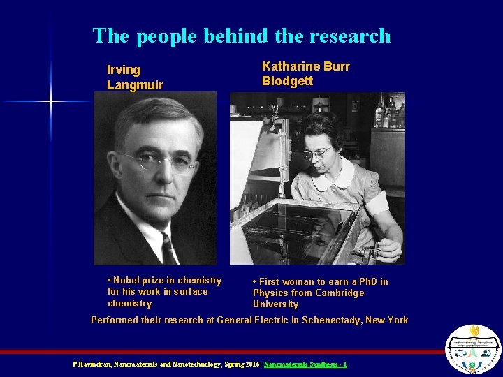
The people behind the research Irving Langmuir • Nobel prize in chemistry for his work in surface chemistry Katharine Burr Blodgett • First woman to earn a Ph. D in Physics from Cambridge University Performed their research at General Electric in Schenectady, New York P. Ravindran, Nanomaterials and Nanotechnology, Spring 2016: Nanomaterials Synthesis - 1

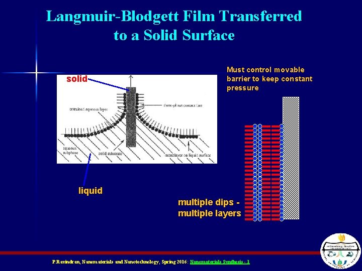
Langmuir-Blodgett Film Transferred to a Solid Surface solid Must control movable barrier to keep constant pressure liquid multiple dips multiple layers P. Ravindran, Nanomaterials and Nanotechnology, Spring 2016: Nanomaterials Synthesis - 1

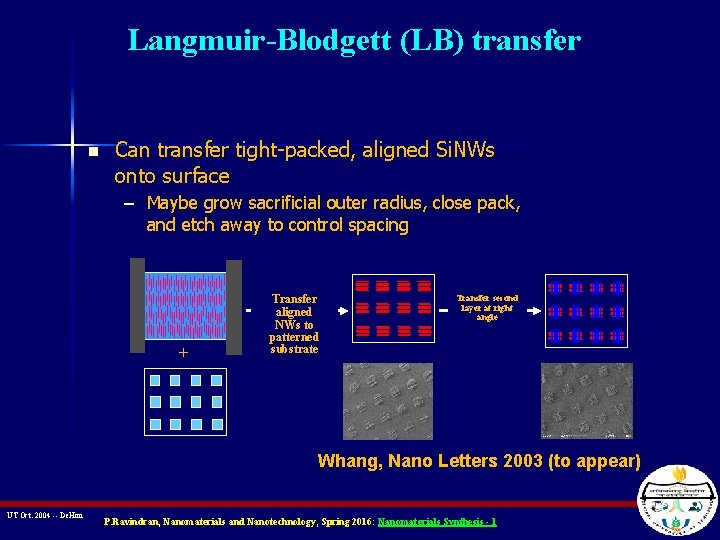
Langmuir-Blodgett (LB) transfer n Can transfer tight-packed, aligned Si. NWs onto surface – Maybe grow sacrificial outer radius, close pack, and etch away to control spacing + Transfer aligned NWs to patterned substrate Transfer second layer at right angle Whang, Nano Letters 2003 (to appear) UT Oct. 2004 -- De. Hon P. Ravindran, Nanomaterials and Nanotechnology, Spring 2016: Nanomaterials Synthesis - 1

Langmuir-Blodgett (LB) Films n n When you dunk the substrate in, you get a monolayer (one layer) of aligned molecules on the substrate If you keep dunking it you’ll get a new layer each time – The water soluble side of one layer aligns with the water soluble side of the next (alternating alignment) P. Ravindran, Nanomaterials and Nanotechnology, Spring 2016: Nanomaterials Synthesis - 1

Langmuir-Blodgett (LB) Films P. Ravindran, Nanomaterials and Nanotechnology, Spring 2016: Nanomaterials Synthesis - 1

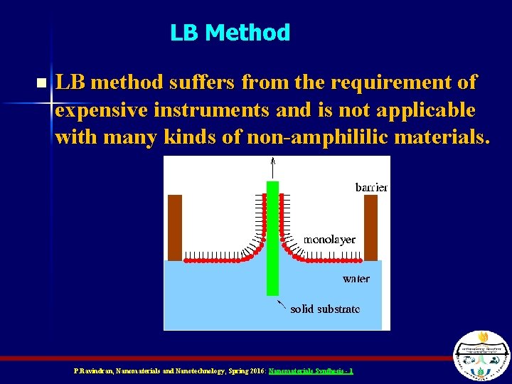
Langmuir-Blodgett (LB) The principle of Langmuir-Blodgett deposition. Amphiphile molecules are spread over the aqueous solution (A). The area of the surface is reduced by the movement of the barriers. This compresses the amphiphiles to form an ordered film (B). The amphiphile film can be transferred to a solid surface if the latter is slowly drawn through the solution/air interface (C). Amphiphile (from the Greek αμφις, amphis: both and φιλíα, philia: love, friendship) is a term describing a chemical compound possessing both hydrophilic (water-loving, polar) and lipophilic (fat-loving) properties. Such a compound is called amphiphilic or amphipathic http: //www. foi. se/surfbiotech/tt/img 00007. gif P. Ravindran, Nanomaterials and Nanotechnology, Spring 2016: Nanomaterials Synthesis - 1

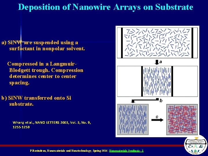
Deposition of Nanowire Arrays on Substrate a) Si. NW are suspended using a surfactant in nonpolar solvent. Compressed in a Langmuir. Blodgett trough. Compression determines center to center spacing. b) Si. NW transferred onto Si substrate. Whang et al. , NANO LETTERS 2003, Vol. 3, No. 9, 1255 -1259 P. Ravindran, Nanomaterials and Nanotechnology, Spring 2016: Nanomaterials Synthesis - 1

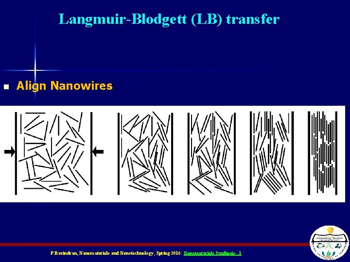
Langmuir-Blodgett (LB) transfer n Align Nanowires P. Ravindran, Nanomaterials and Nanotechnology, Spring 2016: Nanomaterials Synthesis - 1

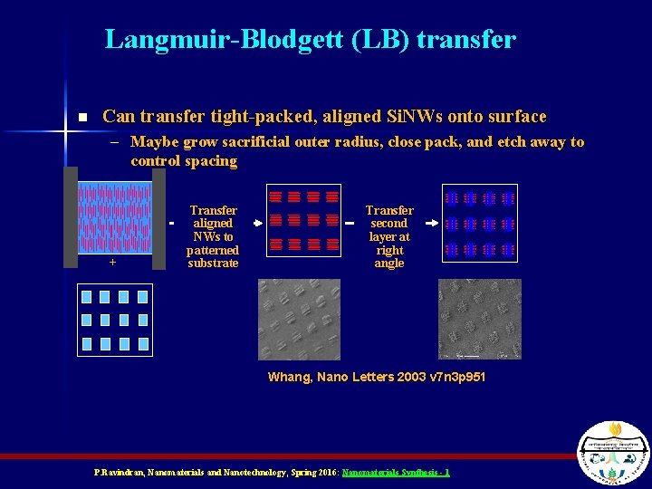
Langmuir-Blodgett (LB) transfer n Can transfer tight-packed, aligned Si. NWs onto surface – Maybe grow sacrificial outer radius, close pack, and etch away to control spacing + Transfer aligned NWs to patterned substrate Transfer second layer at right angle Whang, Nano Letters 2003 v 7 n 3 p 951 P. Ravindran, Nanomaterials and Nanotechnology, Spring 2016: Nanomaterials Synthesis - 1

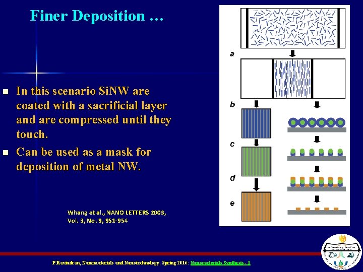
Finer Deposition … n n In this scenario Si. NW are coated with a sacrificial layer and are compressed until they touch. Can be used as a mask for deposition of metal NW. Whang et al. , NANO LETTERS 2003, Vol. 3, No. 9, 951 -954 P. Ravindran, Nanomaterials and Nanotechnology, Spring 2016: Nanomaterials Synthesis - 1

LB Method n LB method suffers from the requirement of expensive instruments and is not applicable with many kinds of non-amphililic materials. P. Ravindran, Nanomaterials and Nanotechnology, Spring 2016: Nanomaterials Synthesis - 1

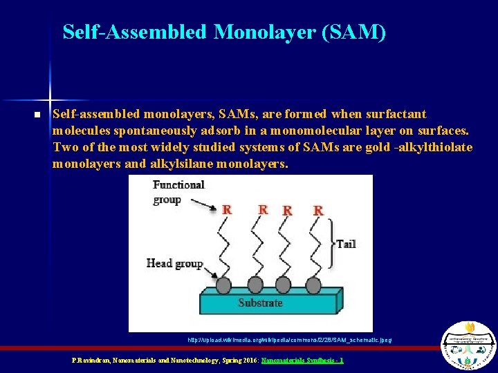
Self-Assembled Monolayer (SAM) n Self-assembled monolayers, SAMs, are formed when surfactant molecules spontaneously adsorb in a monomolecular layer on surfaces. Two of the most widely studied systems of SAMs are gold -alkylthiolate monolayers and alkylsilane monolayers. http: //upload. wikimedia. org/wikipedia/commons/2/28/SAM_schematic. jpeg P. Ravindran, Nanomaterials and Nanotechnology, Spring 2016: Nanomaterials Synthesis - 1

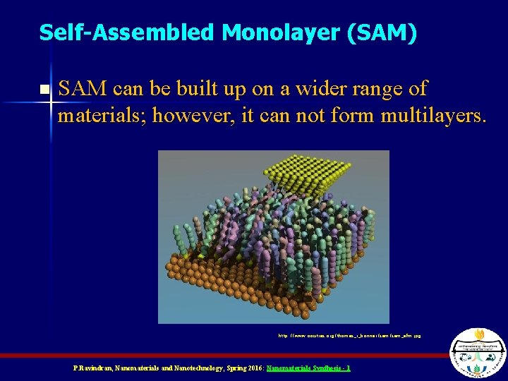
Self-Assembled Monolayer (SAM) n SAM can be built up on a wider range of materials; however, it can not form multilayers. http: //www. oocities. org/thomas_r_bonner/sam_afm. jpg P. Ravindran, Nanomaterials and Nanotechnology, Spring 2016: Nanomaterials Synthesis - 1

Advantages of LBL n (1) LBL is extremely cheap, no expensive instrument required. n (2) The fabrication process is simple, and can be achieved either manually or by machine. n (3) The film can form not only on planar substrates, but also on substrates with different shapes. The thickness increment per layer is self-regulating; similar surface roughness of LBL is expected regardless of the roughness of substrates. n (4) LBL can incorporate different functional groups into the system for different applications. P. Ravindran, Nanomaterials and Nanotechnology, Spring 2016: Nanomaterials Synthesis - 1

Advantages of LBL � (5) Applied materials can be used such as conventional polyelectrolytes as well as various functional polyelectrolytes. � (6) Water-soluble biomaterials with charged sites on their surfaces can also be incorporated, such as proteins, DNA, and charged viruses. � (7) Charged inorganic substances: Colloidal nanoparticles, clay, zeolite and polyoxometalates have been reported for use in LBL assembly. � (8) Charged supramolecular assemblies have also been incorporated into LBL assembly P. Ravindran, Nanomaterials and Nanotechnology, Spring 2016: Nanomaterials Synthesis - 1

Biocompatible LBL films for tissue engineering �Cells are sensitive both to the micro/nano-topographic and chemical features of their surrounding environment. �The engineering of surface properties of biomaterials is critical to develop bioactive devices with which to elicit appropriate cellular responses. ---An example: Development of biocompatible films for bone tissue engineering P. Ravindran, Nanomaterials and Nanotechnology, Spring 2016: Nanomaterials Synthesis - 1

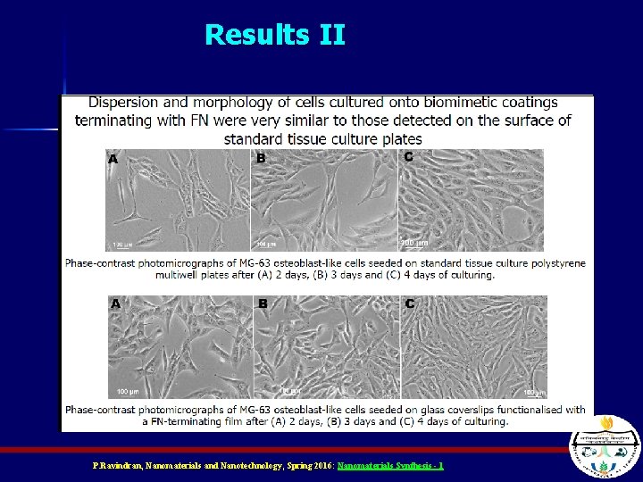
Human Osteoblast-Like Cells Response to Nanofunctionalized Surfaces for Tissue Engineering � Biomimetic coatings containing fibronectin (FN), an adhesive glycoprotein of the extracellular matrix, have been assembled by means of the Lb. L technique. � Three precursor bilayers of cationic poly(dimethyldiallyl ammonium chloride) (PDDA) and anionic poly (styrenesulfonate) (PSS) were deposited to impart an homogeneous and well-defined charge to the substrates. � Subsequently cationic poly-L-lysine (PLL) was employed in alternation with FN. J Biomed Mater Res Part B: Appl Biomater 84 B: 249– 255, 2008 P. Ravindran, Nanomaterials and Nanotechnology, Spring 2016: Nanomaterials Synthesis - 1

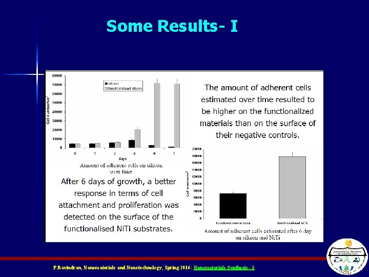
Bone Tissue Engineering �To evaluate the biocompatibility of the developed coatings MG 63 human osteoblast-like cells were used. �Cells were seeded onto functionalised and non functionalized silicon and Nickel/Titanium (Ni. Ti) surfaces. �Cell dispersion and morphology was evaluated on the surface of treated and non treated glass coverslips by phase contrast microscopy. P. Ravindran, Nanomaterials and Nanotechnology, Spring 2016: Nanomaterials Synthesis - 1

Some Results- I P. Ravindran, Nanomaterials and Nanotechnology, Spring 2016: Nanomaterials Synthesis - 1

Results II P. Ravindran, Nanomaterials and Nanotechnology, Spring 2016: Nanomaterials Synthesis - 1

Results II n The developed coatings resulted to be effective in improving cell response both on silicon and Ni. Ti. n These experimental evidences demonstrates the high potential of the assembled ultrathin films for the optimization of the surface properties of bone implants. P. Ravindran, Nanomaterials and Nanotechnology, Spring 2016: Nanomaterials Synthesis - 1

LBL films for Biosensors Development n Multilayer containing functional proteins can be assembled directly onto the surface of a transducer for the setting up of a biosensor MOVIE http: //www. chem. fsu. edu/multilayers/Multilayer%20 Animation%20 Fast. swf P. Ravindran, Nanomaterials and Nanotechnology, Spring 2016: Nanomaterials Synthesis - 1