1 Linear circtuit application Controlled sources VCVS VCCS
 Linear circtuit application - Controlled sources (VCVS, VCCS, CCVS,")
![3. 이상적인 연산 증폭 기 1) 등가회로 <그림> 연산증폭기 등가회로 [www. eeguide. com] 2)](https://slidetodoc.com/presentation_image_h2/b72b916bbccd5274baac48c0d1a5a3ce/image-8.jpg "3. 이상적인 연산 증폭 기 1) 등가회로 <그림> 연산증폭기 등가회로 [www. eeguide. com] 2)")
![4. 비반전 (non-inverting) 연산 증폭 기 <그림> 비반전 증폭기 [www. dummies. com] 1) 전압이득](https://slidetodoc.com/presentation_image_h2/b72b916bbccd5274baac48c0d1a5a3ce/image-9.jpg "4. 비반전 (non-inverting) 연산 증폭 기 <그림> 비반전 증폭기 [www. dummies. com] 1) 전압이득")
![5. 반전 (inverting) 연산 증폭 기 <그림> 비반전 증폭기 [www. dummies. com] 1) 전압이득](https://slidetodoc.com/presentation_image_h2/b72b916bbccd5274baac48c0d1a5a3ce/image-11.jpg "5. 반전 (inverting) 연산 증폭 기 <그림> 비반전 증폭기 [www. dummies. com] 1) 전압이득")
 ㅇ 다른 명칭: In-amp, In. Amp <그림> 계측 증폭기")
, LT 1167 과 동일한 성능을 4 개의 op-amp")
 Frequency-compensate one-pole model ㅇ Open-loop gain - 연산")
 = A(ω) /")

 Q")


- Slides: 32
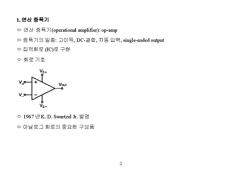
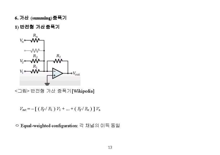
ㅇ 연산 증폭기의 용도 1) Linear circtuit application - Controlled sources (VCVS, VCCS, CCVS, CCCS) - Integrators and differentiators - Summing amps and differencing amps - Variable-gain differential/instrumentation amps - Filters - Oscillators 2) Nonlinear circuit applications - Comparators - Schmitt trigger - Sample and hold circuits - Precision rectifiers - Multivibrators, log-antilog amps, relaxation oscillators 3
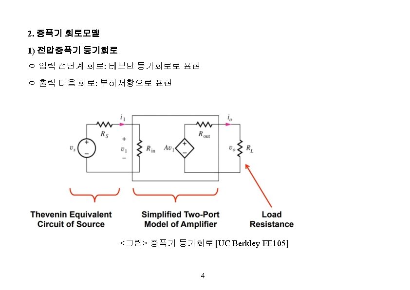
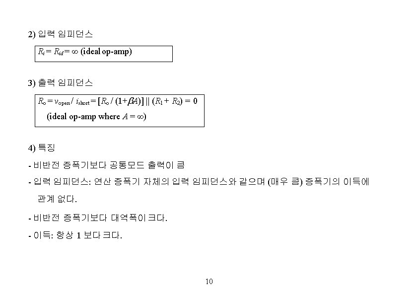
3. 이상적인 연산 증폭 기 1) 등가회로 <그림> 연산증폭기 등가회로 [www. eeguide. com] 2) 이상적인 연산증폭기 특성 A = ∞ (open-loop voltage gain) Ri = ∞ (input impedance) Ro = 0 (output impedance) Ac = 0 (common mode gain): Vo = 0 if Vid = V 2 V 1 = 0 8
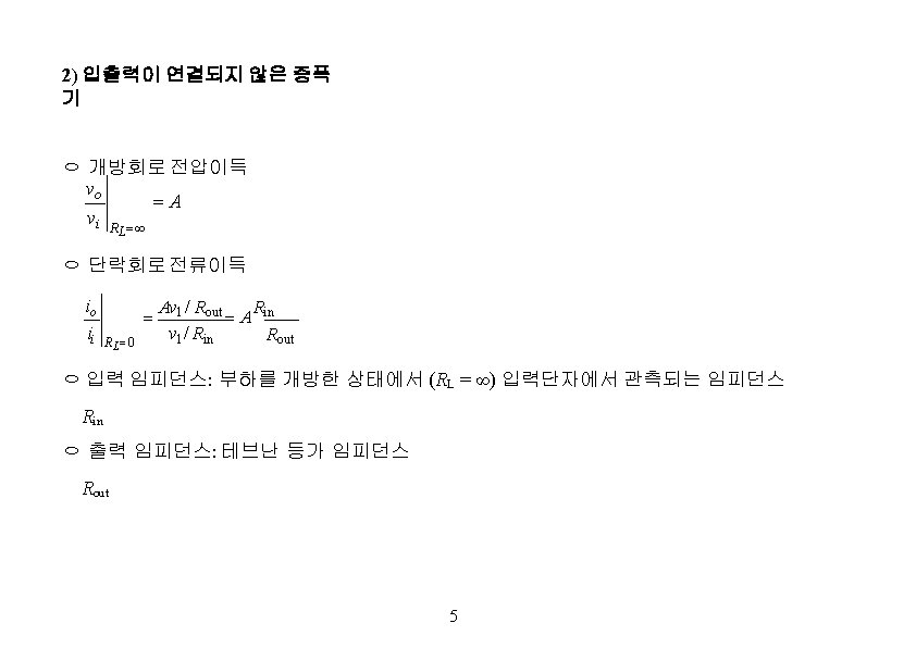
4. 비반전 (non-inverting) 연산 증폭 기 <그림> 비반전 증폭기 [www. dummies. com] 1) 전압이득 ip = 0, i. N = 0, vp = v. N, i 2 = i 1 = i v 0 = (R 1 + R 2) i, i = v 2 / R 1 v 0 = (1 + R 2 / R 1) vs Av = v 0 / vs = 1 + R 2 / R 1 = 1/ = R 1 / (R 1 + R 2) (feedback factor) 9
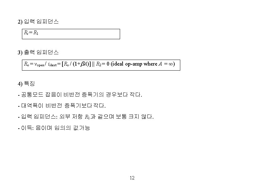
5. 반전 (inverting) 연산 증폭 기 <그림> 비반전 증폭기 [www. dummies. com] 1) 전압이득 v. N = v. P = 0, i. N = 0, i 2 = i 1 = vs / R 1 vo = i 2 R 2 = i 1 R 2 = ( R 2 / R 1) vs Av = v 0 / vs = R 2 / R 1 = (1/ 1) = R 1 / (R 1 + R 2) (feedback factor) 11
7. 계측 증폭기 (Instrumentation Amplifier) ㅇ 다른 명칭: In-amp, In. Amp <그림> 계측 증폭기 [Wikipedia] Av = Vout / (V 2 V 1) = (1 + 2 R 1 /Rgain ) (R 3 / R 2) 17
<그림> LT 1167 monolothic in-amp (right), LT 1167 과 동일한 성능을 4 개의 op-amp 로 구성 (lefrt) [Analog Devices] 19
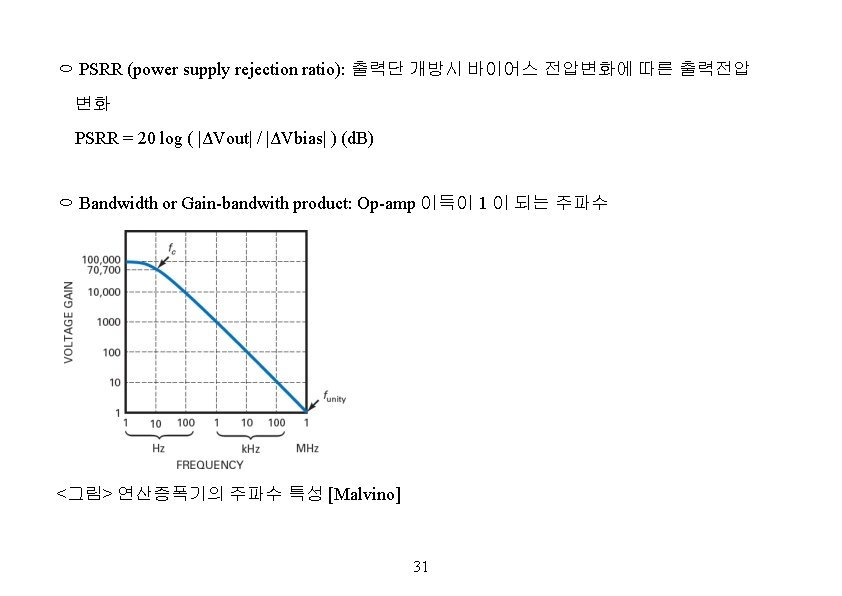
9. 연산 증폭기의 주파수 특성 1) Frequency-compensate one-pole model ㅇ Open-loop gain - 연산 증폭기 자체 이득의 주파수 특성 A(ω) = A(0) / (jω + ωB) ωB : Open-loop bandwidth ωT = A(0) ωB >> ωB : Unity-gain frequency = Gain-bandwidth product 21
ㅇ Closed-loop gain - 궤환 연산 증폭기 이득의 주파수 특성 Av(ω) = A(ω) / [1 + A(ω)] = Av(0) / (1 + jω/ωH) ωH = [1 + A(0)] ωB : Closed-loop bandwidth ωT = A(0) ωB >> ωB : Unity-gain frequency = Gain-bandwidth product <그림> 연산 증폭기 주파수 특성 [A. Doolittle] 22
ㅇ Gain-bandwidth product = Constant Gain × Bandwidth |Open Loop = Gain × Bandwidth |Closed. Loop A(0) f. B = Av(0) f. H 23
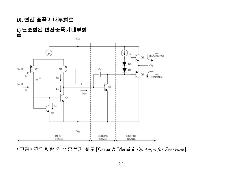
Q 1, Q 2: 차동증폭기, transconductance amplifier Iout 1 = gm (Vp Vn) Q 3, Q 4: Current mirror for Q 1, Q 2. Q 4 의 컬렉터 전류가 항상 Ic 1 과 같게 유지. Iout 1 = Ic 2 Ic 1 Q 5: Transresistance amplifier, common emitter 증폭기 Cc: Compensation feedback capacitor for gain roll-off versus frequency. Prevents the op-amp from oscillation. Q 6, Q 7: Current amplifier with unity voltage gain. Push-pull amplifier 25
ㅇ Offset current Iio: 출력단 개방시 입력단자로 흘러들어가는 전류 Ibias = ( IB+ + IB ) / 2 (바이어스 전류) Iio = IB+ IB (오프셋 전류) ㅇ CMRR (common-mode rejection ratio): CMRR = 20 log ( | G 0 | / | Gcm | ) (d. B) 30
ㅇ Slew rate - 출력신호의 응답속도 SR = max ( | dvo / dt | ) SR = Ibias / CC CC : frequency-compenstation capacitor inside op amp Ibias : 바이어스 전류 - Large output voltage and/or high frequencies - Slew-induced signal distortion - 연산증폭기 최대 동작주파수: Slew rate 에 의해 결정됨. fmax = SR / [2π vo, max]: FPBW (full power bandwidth) v 0 (t) = Vp sin (ωt) SR = 2 π f Vp fmax = SR / (2πVp) - Gain-bandwidth product 에 의해 결정되는 small signal 주파수 대역보다 slew rate 에 의해 결정되는 대역폭이 훨씬 작음. 32