1 Digital System What Why How 2 Binary
 1. Digital System: What? Why? How? 2. Binary Logic &")
조합논리회로의 해석과 설계 (복습) 1. Digital System: What? Why? How? 2. Binary Logic & Gates 3. Boolean Algebra: Definition, Theorems 4. Boolean Expression: 분류, ⇔ Logic Diagram 5. Map Simplification: Karnaugh Map 6. Other Logic Gates 7. 조합논리회로의 해석 8. 조합논리회로의 설계 9. Combinational Functional Blocks: Encoder, Decoder, Multiplexer, Demultiplexer, Code converter, Adder, Subtractor, Adder/Subtractor, Multiplier, … ⓒ 2006 B. G. KIM 디지털시스템 3

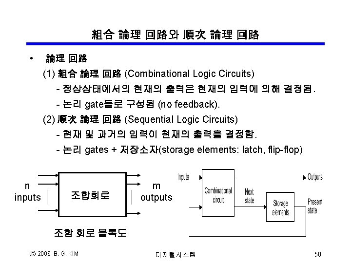
1. Digital System: What? Why? How? § Digital system ≡ a system that processes (stores, communicates, transforms/manipulates) information expressed in discrete(離散) form. (예) general-purpose digital computers, … § Digital signal ≡ signal with discrete meaningful states(values). ↔ analog signal § Digital over Analog: Reliability(信賴性) ≪ high noise immunity § Analog to Digital: Quantization and Encoding Digital signals for analog information (or signal)? ⇒ quantization(量子化) in both value and time Binary signals for multivalued information? ⇒ encoding(符號化) : BCD code, ASCII code, Excess-3 code § Coding? ⇒ What to do with that code? 效果와 效率 ⓒ 2006 B. G. KIM 디지털시스템 4
: 논리회로의 기본 수학 - Binary")
2. BINARY LOGIC & GATES 1. Binary Logic (2進論理): 논리회로의 기본 수학 - Binary Logic ⊆ Boolean Algebra Switching algebra, Two-valued Boolean Algebra 2値부울代數 {참, 거짓}n {HIGH, LOW}n {참, 거짓} 2진 디지털 시스템 {ON, OFF}n {HIGH, LOW} {ON, OFF} 논리학: 접속사 and, or, not Switch 회로: 직렬연결, 병렬연결, NC/NO switch {? ? , ? ? }n 수학적 모델 {? ? , ? ? } ? ? , ? ? ⓒ 2006 B. G. KIM 디지털시스템 5

2. BINARY LOGIC & GATES 2. Three Basic Logical Operations 2진 디지털 시스템 기술에 필요, 충분한 연산(동작)의 수와 종류는? 2진논리 2진 시스템 1 -bit 2진수 연산 (Binary Logic) (Binary Digital System) (1 -bit Binary Arithmetic) ⓒ 2006 B. G. KIM 디지털시스템 6
 Logic Gates = 2진 논리를 수행하는 단위")
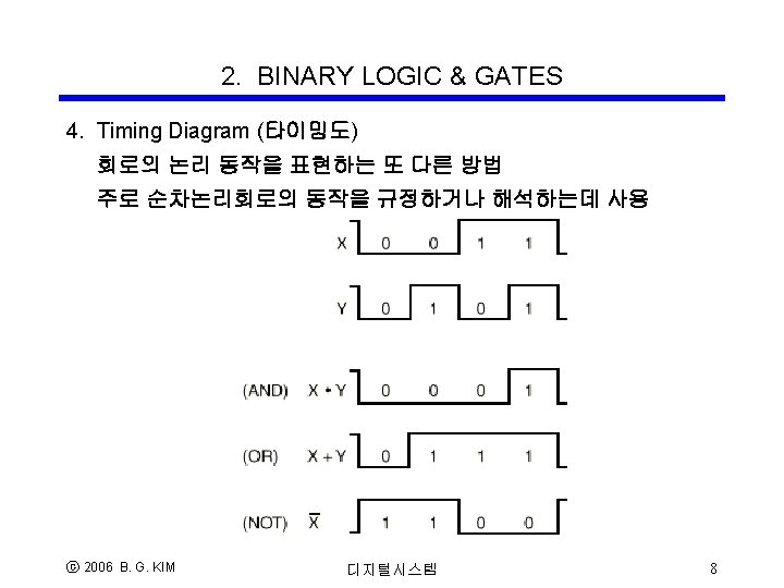
2. BINARY LOGIC & GATES 3. (Basic) Logic Gates = 2진 논리를 수행하는 단위 전자회로 ⓒ 2006 B. G. KIM 디지털시스템 7
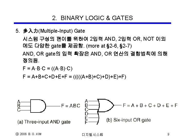
 2. Huntington의 부울 代數의 假說: < V={…}, O={+, .")
3. BOOLEAN ALGEBRA (부울 代數) 2. Huntington의 부울 代數의 假說: < V={…}, O={+, . } > 1. (a) V is closed with respect to the operation p 1. (b) V is closed with respect to the operation p 2. 2. (a) V has an identity element w. r. t the operation p 1. (b) V has an identity element w. r. t the operation p 2. 3. (a) V is commutative w. r. t the operation p 1. (b) V is commutative w. r. t the operation p 2. 4. (a) p 1 is distributive over p 2. (b) p 2 is distributive over p 1. 5. For each x in V, there exists an element y in V such that (a) x + y = 1 (b) x. y = 0 6. |V| ≥ 2 ⓒ 2006 B. G. KIM 디지털시스템 11
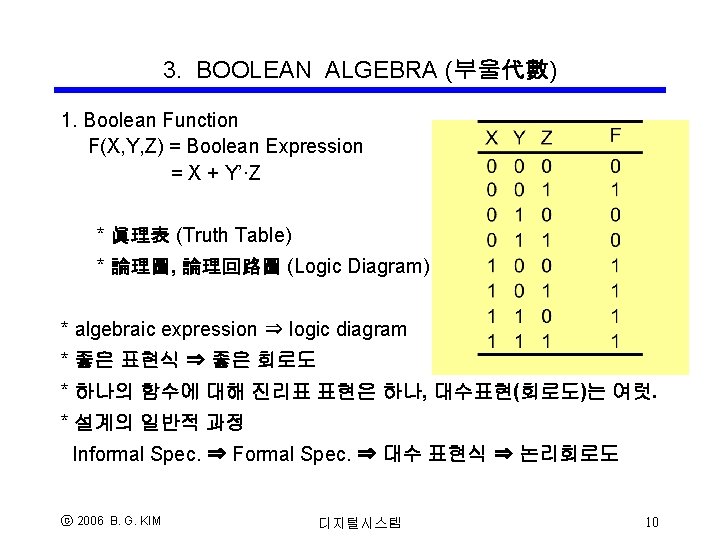
 3. Basic Identities of Boolean Algebra 1) X + 0")
3. BOOLEAN ALGEBRA (부울代數) 3. Basic Identities of Boolean Algebra 1) X + 0 = X 2) X· 1 = X 恒等元(identity) (公理) 3) X + 1 = 1 4) X· 0 = 0 Identity Theorem 恒等元 定理 5) X + X = X 6) X·X = X Idempotence Th. 冪等의 定理 7) X + X’ = 1 8) X·X’ = 0 補元(Complement ) 9) (X’)’ = X 10) X + Y = Y + X Involution Th. 累乘 定理 11) X·Y = Y·X Commutative Law 12) X+(Y+Z) = (X+Y)+Z 13) X·(Y·Z) = (X·Y)·Z Associative Law 14) X·(Y + Z) = X·Y+ X·Z 15) X + Y·Z = (X+Y)·(X+Z) Distributive Law 16) (X + Y)’ = X’·Y’ 17) (X·Y)’ = X’ + Y’ De Morgan’s Th. * 일반 대수와의 차이? 역원(inverse)? * 雙對性 原理(Principles of Duality): AND↔OR, 0↔ 1 ⓒ 2006 B. G. KIM 디지털시스템 12
 Key Points: 부울 표현식의 형태 분류, 관련 용어, 형태")
4. BOOLEAN EXPRESSION (부울 표현식) Key Points: 부울 표현식의 형태 분류, 관련 용어, 형태 사이의 변환 1. 부울표현식의 형태 - 標準型(Standard Form): 곱의 합형(Sum-of-Products, SOP, or Disjunctive Form) F(X, Y, Z) = XY + X’Z + YZ 합의 곱형(Product-of-Sums, POS, or Conjunctive Form) F(X, Y, Z) = (X + Y)(X’ + Z)(Y + Z) - 非標準型(Non-standard, Factored, or Parenthesized Form) F(X, Y, Z) = X’ + (Y + Z)(Y’ + Z’) - 正型(Canonical Form): 표준형의 특별한 경우 곱의합 정형(Canonical SOP, or Canonical Disjunctive Form) F(X, Y, Z) = XYZ + XYZ’ + X’YZ [sum-of-minterms form] 합의곱 정형(Canonical POS, or Canonical Conjunctive Form) F(X, Y, Z) = (X+Y+Z)(X+Y+Z’) [product-of-maxterms form] * 한 함수에 대한 정형 표현식은 唯一함. ⓒ 2006 B. G. KIM 디지털시스템 15
 * 곱항(product term) = ANDing of literals * 합항(sum")
4. BOOLEAN EXPRESSION (부울 표현식) * 곱항(product term) = ANDing of literals * 합항(sum term) = ORing of literals * 표준형 = 2段階 표현식(Two-Level Form) * 비표준형 = 多段階 표현식(Multi-Level Form) 2. Minterms and Maxterms - minterm(最小項, 最小積項, 標準積 standard product) = a product term in which all the variables appear exactly once, either complemented or uncomplemented. - maxterm(最大項, 最大合項, 標準合 standard sum) = a sum term in which all the variables appear exactly once, either complemented or uncomplemented. * The order of the variables should be assumed for the symbolic representation of minterms/maxterms. ⓒ 2006 B. G. KIM 디지털시스템 16
 Table 2 -6 Minterms for Three Variables ⓒ 2006")
4. BOOLEAN EXPRESSION (부울 표현식) Table 2 -6 Minterms for Three Variables ⓒ 2006 B. G. KIM 디지털시스템 17
 Table 2 -7 Maxterms for Three Variables ⓒ 2006")
4. BOOLEAN EXPRESSION (부울 표현식) Table 2 -7 Maxterms for Three Variables ⓒ 2006 B. G. KIM 디지털시스템 18
 3. Canonical Expressions - sum-of-minterms of F and F’")
4. BOOLEAN EXPRESSION (부울 표현식) 3. Canonical Expressions - sum-of-minterms of F and F’ F(X, Y, Z) = […] + … = X’Y’Z’ + X’YZ’ + XY’Z + XYZ = m 0 + m 2 + m 5 + m 7 = Sm(0, 2, 5, 7), or S(0, 2, 5, 7) F’(X, Y, Z) = […] + … = X’Y’Z + X’YZ + XY’Z’ + XYZ’ = m 1 + m 3 + m 4 + m 6 = Sm(1, 3, 4, 6), or S(1, 3, 4, 6) ⓒ 2006 B. G. KIM 디지털시스템 19
 - product-of-maxterms of F and F’ F(X, Y, Z)")
4. BOOLEAN EXPRESSION (부울 표현식) - product-of-maxterms of F and F’ F(X, Y, Z) = (…)·(…)·… = (X+Y+Z’)(X+Y’+Z’)(X’+Y+Z)(X’+Y’+Z) = M 1·M 3·M 4·M 6 = PM(1, 3, 4, 6), or P(1, 3, 4, 6) Similarly, F’(X, Y, Z) = M 0·M 2·M 5·M 7 = P(0, 2, 5, 7) Another method: F’(X, Y, Z) = [F(X, Y, Z)]’ = (m 0 + m 2 + m 5 + m 7)’ = (m 0)’·(m 2)’·(m 5)’·(m 7)’ = M 0·M 2·M 5·M 7 = P(0, 2, 5, 7) ⓒ 2006 B. G. KIM 디지털시스템 F(·) = S(0, 2, 5, 7) = P(1, 3, 4, 6) F’(·) = S(1, 3, 4, 6) = P(0, 2, 5, 7) 20
 5. Sum of Products - sum-of-minterms. obtained directly from")
4. BOOLEAN EXPRESSION (부울 표현식) 5. Sum of Products - sum-of-minterms. obtained directly from a truth table. the most complex sum-of-products form. but, a starting point to a simplified s-o-p form - logic diagram of a s-o-p form? . two-level, AND-OR, implementation. (complements of input variables are assumed to be available) - Non-standard form to SOP form? . by means of the distributive law - SOP to simplified SOP? . many ways. Simplification Th. , Consensus Th. , Identity Th. , …. - Figure 2 -5, Figure 2 -6 ⓒ 2006 B. G. KIM 디지털시스템 22
 - 다단계회로와 2단계회로 (Figure 2 -6) 6. Product of")
4. BOOLEAN EXPRESSION (부울 표현식) - 다단계회로와 2단계회로 (Figure 2 -6) 6. Product of Sums - Two-level, OR-AND Implementation - Figure 2 -7 ⓒ 2006 B. G. KIM 디지털시스템 23

5. MAP SIMPLIFICATION What to Study: Map method for logic simplification 맵 방법에 의한 논리 (표현식) 최소화/간소화 1. Simplification Criterion: 최소화/간소화된 곱의합 표현이란? F = (…) + … + (…) (i) with a minimum number of terms (ii) with the fewest possible number of literals * There may be many, equally good expressions! 2. 대수적 간소화(Algebraic Simplification) 과정의 예 f(a, b, c) = a’b’c’ + a’b’c + a’bc’ + a’bc + abc = ⓒ 2006 B. G. KIM a’b’ + a’b + abc = a’ + bc 디지털시스템 24
 = a’b’c’ + a’b’c + a’bc’ + a’bc")
5. MAP SIMPLIFICATION f(a, b, c) = a’b’c’ + a’b’c + a’bc’ + a’bc + abc = a’b’ + a’bc’ + bc = a’(b’ + bc’) + bc = a’(b’ + c’) + bc = a’b’ + a’c’ + bc = a’(bc)’ + bc = a’ + bc f(a, b, c) = a’b’c’ + a’b’c + a’bc’ + a’bc + abc = a’b’ + a’b + bc = a’ + bc = ? ? ? * With proper duplication of product terms, only the distributive law would do the job. ⓒ 2006 B. G. KIM 디지털시스템 25
")
5. MAP SIMPLIFICATION 3. Algebraic Simplification: Use any boolean axioms and theorems, or (1) two adjacent product terms into one bigger product term (2) a term may be used more than once during combination (3) a term may be partitioned into smaller ones But, still we have some difficulties: (1) no specific rules to predict each succeeding step (2) difficult to determine whether the simplest expression has been achieved - Simplify the following expression: f(A, B, C, D) = A’BC’D + A’BCD + ABC’ + ABCD + A’BCD’ = A’BD + ABC’ + ABCD + A’BCD’ = …… ? ? ? = ABC’ + A’BC + BD ⓒ 2006 B. G. KIM 디지털시스템 26
 (1) 진리표의 2차원적 그림 표현")
5. MAP SIMPLIFICATION 4. Karnaugh Map, (K-map, Veitch Diagram) (1) 진리표의 2차원적 그림 표현 (인접관계를 시각적으로 판단 가능) (2) 인접한 최소항 또는 곱항끼리 물리적으로도 가까이 있도록 배치 (3) 수작업에 의한 간소화에 사용 (not for computer-aided design) (4) 곱의합 또는 합의곱 형태 간소화에 사용 (not apply directly to simplification in non-standard forms) (5) up to 4 variables? ==> depends on YOU! Glue logic * possible to find two or more simplified expressions. ⓒ 2006 B. G. KIM 디지털시스템 27

5. MAP SIMPLIFICATION 5. 2 -, 3 -, 4 -Variable K-Maps * Gray Code Y XY Z 0 1 0 X’Y’ X’Y X 1 XY’ XY Y 0 0 1 0 0 0 1 XY Z 0 0 1 1 1 0 0 X 1 0 1 0 m 1 X 1 m 2 m 3 Y 0 1 0 0 1 X 1 2 3 ⓒ 2006 B. G. KIM 0 0 1 1 0 1 Y Y 0 1 X 1 1 1 0 Note the adjacency of minterms 디지털시스템 28

5. MAP SIMPLIFICATION Y 01 00 11 Y 10 Y 00 01 11 10 0 0 m 1 m 3 m 2 0 0 1 3 2 X 1 m 4 m 5 m 7 m 6 X 1 4 5 7 6 Z Z Z Y 00 01 11 10 W 00 0 1 3 2 01 4 5 7 6 11 12 13 15 14 10 8 9 11 10 X Z ⓒ 2006 B. G. KIM 디지털시스템 29
![5. MAP SIMPLIFICATION [EXAMPLE 2 -6] C 00 01 11 10 00 01 A](http://slidetodoc.com/presentation_image_h/d71f683f809be864ac97e06b0c469e06/image-30.jpg "5. MAP SIMPLIFICATION [EXAMPLE 2 -6] C 00 01 11 10 00 01 A")
5. MAP SIMPLIFICATION [EXAMPLE 2 -6] C 00 01 11 10 00 01 A B 11 10 D ⓒ 2006 B. G. KIM 디지털시스템 30
 합의곱")
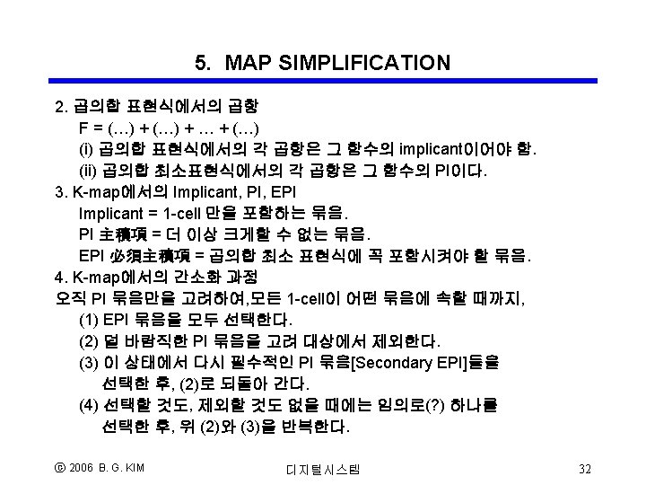
5. MAP SIMPLIFICATION What to Study: 맵 방법에 의한 논리 최소화 (체계적 방법) 합의곱 표현의 최소화 無關條件(Don’t-Care Conditions)이 있는 경우 1. Implicant, Prime Implecant, Essential Prime Implicant F = (…) + (…) - Implicant = a product term if the function has the value 1 for all minterms of the product term, 즉, 주어진 함수의 곱의합 표현에 나타날 수 있는 곱항. - Prime Implicant(PI) 主積項 = 문자를 더 이상 줄일 수 없는 implicant, 다른 implicant에 포함되지 않는 implicant. - Essential Prime Implicant (EPI) 必須主積項 = 어떤 최소표현식에 도 항상 포함되어야 하는 주적항. ⓒ 2006 B. G. KIM 디지털시스템 31
![5. MAP SIMPLIFICATION [Examples] C C 00 01 11 10 A 00 1 1](http://slidetodoc.com/presentation_image_h/d71f683f809be864ac97e06b0c469e06/image-33.jpg "5. MAP SIMPLIFICATION [Examples] C C 00 01 11 10 A 00 1 1")
5. MAP SIMPLIFICATION [Examples] C C 00 01 11 10 A 00 1 1 01 1 11 1 D ⓒ 2006 B. G. KIM 00 01 11 10 00 1 10 C B A 01 1 1 B 1 10 1 D 디지털시스템 1 A 00 1 1 01 1 1 1 B 1 10 1 1 D 33
 (1) F’의 s-o-p를 구하여 양변의 complement를")
5. MAP SIMPLIFICATION 5. Product-of-Sums Simplification (합의곱형 간소화) (1) F’의 s-o-p를 구하여 양변의 complement를 취함. (2) F의 K-map에서 0 -cell을 grouping함. [Grouping한 조건들을 합항으로 표현할 때, 문자의 극성에 주의] [Example 2 -8] F(A, B, C, D) = S(0, 1, 2, 5, 8, 9, 10) C 00 01 11 10 A 00 1 1 01 0 0 11 0 0 10 1 1 0 1 B D ⓒ 2006 B. G. KIM 디지털시스템 34
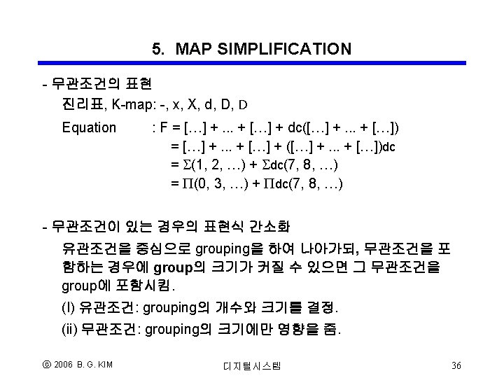
 = 함수의 출력이 정의되지 않은 입력 조건들.")
5. MAP SIMPLIFICATION 6. Don’t-Care Conditions (無關條件) = 함수의 출력이 정의되지 않은 입력 조건들. (i) the input combinations never occur. (ex) BCD code (ii) the input combinations would occur, but we do not care about the outputs in response to these combinations. => We simply do not care what value is assumed by the function for the unspecified conditions. * imcompletely specified functions (불완전하게 정의된 함수) - What shall we do with DC conditions? DC 조건에 대한 함수의 출력은 설계자가 임의로 설정 가능. But, somebody will get better designs!! How many complete specifications are possible for a 4 -input 1 -output function with 6 DC conditions? ==> ⓒ 2006 B. G. KIM 디지털시스템 35
![5. MAP SIMPLIFICATION [Example] F(A, B, C, D) = S(1, 3, 7, 11, 15)](http://slidetodoc.com/presentation_image_h/d71f683f809be864ac97e06b0c469e06/image-37.jpg "5. MAP SIMPLIFICATION [Example] F(A, B, C, D) = S(1, 3, 7, 11, 15)")
5. MAP SIMPLIFICATION [Example] F(A, B, C, D) = S(1, 3, 7, 11, 15) + Sdc(0, 2, 5) C 00 01 11 10 A 00 x 1 1 x 01 0 x 1 0 11 0 0 10 0 0 1 0 B D ⓒ 2006 B. G. KIM 디지털시스템 37

6. OTHER LOGIC GATES What to study: NAND와 NOR gate를 이용한 부울함수 具現 1. AND, OR, NOT 이외에 다른 type의 gate들이 제공됨. Gate type을 결정할 때의 고려 사항: - feasibility & economy of the gates in the implementation tech. - possibility of fan-in extension - ability to implement Boolean functions 2. Simple Gate Types in Bipolar and CMOS Technology: names(이름), graphic symbols(회로 기호), functions(기능) [Figure 2 -26] in next slide * negation indicator, bubble ⓒ 2006 B. G. KIM 디지털시스템 38

6. OTHER LOGIC GATES ⓒ 2006 B. G. KIM 디지털시스템 39

6. OTHER LOGIC GATES ⓒ 2006 B. G. KIM 디지털시스템 40
 Completeness 函數的(論理的) 完全性 A set of gates are")
6. OTHER LOGIC GATES 3. Functional(Logical) Completeness 函數的(論理的) 完全性 A set of gates are functionally, or logically complete if any Boolean function can be implemented or expressed using only the gate types in the set: {AND, OR, NOT} is functionally complete. {NAND} and {NOR} are functionally complete. [PROVE? => Figure 2 -27, Figure 2 -33 below] *Universal Gates ⓒ 2006 B. G. KIM 디지털시스템 41

6. OTHER LOGIC GATES 4. How to implement a Boolean function with NAND gates? (1) Obtain the simplified expression and/or circuit in terms of AND, OR, and NOT. (2) Convert AND, OR, NOT gates to NAND gates. [bubble insertion] more on later slides Alternative NAND and NOT Symbols for Conversion [Fig. 2 -28] ⓒ 2006 B. G. KIM 디지털시스템 42

6. OTHER LOGIC GATES 5. Two-Level NAND Circuits - NAND-NAND Two-Level Implementation - S-O-P expression can be realized by NAND-NAND circuits Figure 2 -29 for the circuits and also for the conversion from AND -OR using bubble insetion. [Example 2 -9 & Fig. 2 -30] F(x, y, z) = S(1, 2, 3, 4, 5, 7) 을 NAND gates로 구현하라. (1) Simplify in sum-of-products form (2) Draw AND-OR network (Use buffer for terms with single literal) (3) Convert it into NAND-NAND network ⓒ 2006 B. G. KIM 디지털시스템 43

6. OTHER LOGIC GATES 6. NOR Circuits Can repeat the disscussion with NAND circuits. Alternative Symbols for NOR [Fig. 2 -34] NOR-NOR form = P-O-S expression [Fig. 2 -35] Converting AND/OR Circuits into NOR Circuits [Fig. 2 -36] ⓒ 2006 B. G. KIM 디지털시스템 44

6. OTHER LOGIC GATES ⓒ 2006 B. G. KIM 디지털시스템 45

6. OTHER LOGIC GATES 1. Exclusive-OR 함수: XOR, EOR - X Å Y = X·Y’ + X’·Y [difference ftn. ] 2. Exclusive-NOR 함수: XNOR, ENOR - complement of exclusive-or - (X Å Y)’ = X’·Y’ + X·Y [equivanlece ftn] ⓒ 2006 B. G. KIM 디지털시스템 46

![6. OTHER LOGIC GATES 4. XOR Gate의 NAND 구현: [Fig. 2 -37] 5. 다변수](http://slidetodoc.com/presentation_image_h/d71f683f809be864ac97e06b0c469e06/image-48.jpg "6. OTHER LOGIC GATES 4. XOR Gate의 NAND 구현: [Fig. 2 -37] 5. 다변수")
6. OTHER LOGIC GATES 4. XOR Gate의 NAND 구현: [Fig. 2 -37] 5. 다변수 XOR - A Å B Å C = ? ? ? - Odd function (홀수 함수) : F = 1 when … - K-map for XORs: check board : [Fig. 2 -38] - Multiple-Input XOR with 2 -Input XOR: [Fig. 2 -39] - 응용 예: Parity 생성과 검출 ⓒ 2006 B. G. KIM 디지털시스템 48

Gates as Control Elements • Gate as Operators • Gate as Control Elements ⓒ 2006 B. G. KIM 디지털시스템 49

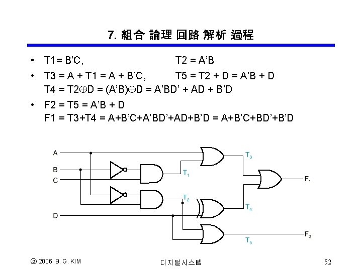
7. 組合 論理 回路 解析 過程 • Determine the function that the given circuits implements: - Logic diagrams => Boolean functions => explanation - manual, logic simulation • Boole 표현식 유도 1. Label all the intermediate signals. 2. Usually from PI(Primary Input) to PO(Primary Output). • 진리표 유도 1. From Boolean functions, or 2. Directly from the logic diagram. (from PI to PO again) • Logic Simulation - fast and accurate: logic waveforms, truth tables - not usually produce Boolean equations - input: net list, schematic input stimulus (vector or waveform) ⓒ 2006 B. G. KIM 디지털시스템 51
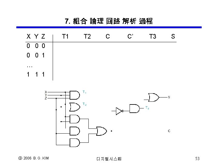

7. 組合 論理 回路 解析 過程 Computer Simulation * propagation delays 전달 지연 시간, gate delay ⓒ 2006 B. G. KIM 디지털시스템 54

8. 組合 論理 回路 設計 過程 • Design Procedure 1. From spec. , determine # and symbols of input and outputs. 2. Derive the truth table. 3. Obtain the simplified Boolean functions for each output. (2단계 표현식, 2단계표현식⇒다단계표현식) 4. Draw the logic diagram. 5. Verify the correctness of the design. * For multiple-output circuits? * For multi-level circuits? * With gates in a library given? ⓒ 2006 B. G. KIM 디지털시스템 55
![8 -1 BCD-to-Excess-3 Code Converter [設計 例] BCD-to-Excess-3 Code Converter ⓒ 2006 B. G.](http://slidetodoc.com/presentation_image_h/d71f683f809be864ac97e06b0c469e06/image-56.jpg "8 -1 BCD-to-Excess-3 Code Converter [設計 例] BCD-to-Excess-3 Code Converter ⓒ 2006 B. G.")
8 -1 BCD-to-Excess-3 Code Converter [設計 例] BCD-to-Excess-3 Code Converter ⓒ 2006 B. G. KIM 디지털시스템 56

8 -1 BCD-to-Excess-3 Code Converter ⓒ 2006 B. G. KIM 디지털시스템 57
 X = B’C+B’D+BC’D’ =")
8 -1 BCD-to-Excess-3 Code Converter W = A+BC+BD = A+B(C+D) X = B’C+B’D+BC’D’ = B’(C+D)+BC’D’=B’(C+D)+B(C+D)’=BÅ(C+D) Y = CD+C’D’ = (CÅD)’ = ((C+D)(C’+D’))’ = CD + (C+D)’ Z = D’ ⓒ 2006 B. G. KIM 디지털시스템 58
![8 -2 BCD-to-Seven-Segment Decoder [設計 例] BCD-to-Seven-Segment Decoder ⓒ 2006 B. G. KIM 디지털시스템](http://slidetodoc.com/presentation_image_h/d71f683f809be864ac97e06b0c469e06/image-59.jpg "8 -2 BCD-to-Seven-Segment Decoder [設計 例] BCD-to-Seven-Segment Decoder ⓒ 2006 B. G. KIM 디지털시스템")
8 -2 BCD-to-Seven-Segment Decoder [設計 例] BCD-to-Seven-Segment Decoder ⓒ 2006 B. G. KIM 디지털시스템 59

8 -2 BCD-to-Seven-Segment Decoder • Minimizing each output separately: => 26 AND gates. 1 1* 1 1* ⓒ 2006 B. G. KIM 1 1 1* 1* 1 1 1* 1 1* 1* 1 1 1* 디지털시스템 60

8 -2 BCD-to-Seven-Segment Decoder • Minimizing each output separately, then simply sharing the same gates: => 15 AND gates 1 1* 1 1* ⓒ 2006 B. G. KIM 1 1 1* 1* 1 1 1* 1 1* 1* 1 1 1* 디지털시스템 61

8 -2 BCD-to-Seven-Segment Decoder • Minimizing each output separately, then simply sharing the same gates, then reduce PI to non-PI for sharing: => 12 AND gates 1 1* 1 1* ⓒ 2006 B. G. KIM 1 1 1* 1* 1 1 1* 1 1* 1* 1 1 1* 디지털시스템 62

8 -2 BCD-to-Seven-Segment Decoder • More aggressive minimization: => 9 AND gates: 1 1 1* 1 1* ⓒ 2006 B. G. KIM 1 1 1* 1 1 1 1 1 디지털시스템 1 1 1* 1* 1 1 1 63

9. Combinational MSI’s & LSI’s • Ultimate Goal of System Design - low cost over the product life of the system - design cost <= time & labor <= design automation manufacturing cost <= parts & labor, production volume maintenance cost <= reliable design • How to select parts? - use standardized component: standardization => mass production & second sources => low cost, high reliability, uninterrupted supply - use bargain components: MSI and LSI over SSI. - choose components for future cost => Use MSI and LSI standard components as much as possible. (Use it directly or with a little modification using extra gates. ) ⓒ 2006 B. G. KIM 디지털시스템 64

9. Combinational MSI’s & LSI’s • What kinds of MSI and LSI Circuits? (Refer to commercial data books. ) - Combinational Circuits: multiplexer, decoder, encoder, demultiplexer, adder-subtractor, look-ahead carry generator, parity generator/checker, 7 -segment driver, comparator, multiplier, ALU, … ROM, PLD(PROM, PLA, PAL, FPGA, …) - Sequential Circuits: counter, shift register, … • What to study for MSI’s? - function (external operation) - extension of data width ⓒ 2006 B. G. KIM - internal organization - other applications 디지털시스템 65
 selected")
9 -1 DECODERS • Function and Internal Structure: inverse of coding - output(s) selected by the input code are active, - input/output polarity (active HIGH/LOW)? - signals on unselected outputs (inactive state, or tri-state)? - enable signals & their polarity? 7442 7447 A 7448 74154 74156 BCD-to-Decimal Decoder BCD-to-Seven-Segment Decoder/Driver (active LOW) BCD-to-Seven-Segemnt Decoder/Driver (active HIGH) 4 -Line to 16 -Line Decoder/Demultiplexer Dual 2 -Line to 4 -Line Decoder/Demultiplexer n input lines ⓒ 2006 B. G. KIM m n-to-m decoder output (n≤m≤ 2 n) lines 디지털시스템 66

9 -1 DECODERS Table 3 -4 Truth Table for 3 -to-8 Line Decoder ⓒ 2006 B. G. KIM 디지털시스템 67

9 -1 DECODERS Fig 3 -12: 3 -to-8 Line Decoder ⓒ 2006 B. G. KIM 디지털시스템 68

9 -1 DECODERS Fig 3 -13: 2 -to-4 Line Decoder with Enable Input D 3 A 1 (active low output) D 2 D 1 A 0 E ⓒ 2006 B. G. KIM 디지털시스템 D 0 69

9 -1 DECODERS • Decoder Expansion: 3 -to-8 Line Decoder with Two 2 -to-4 Decoders [Q] An enable input is a must for decoder expansion? ⓒ 2006 B. G. KIM 디지털시스템 70

9 -1 DECODERS • Combinational Circuit Implementation A decoder provides the 2 n minterms of n input variables. Any Boolean function can be expressed as a sum of minterms. => Any n-input m-output combinational circuit can be implemented with an n-to-2 n-line decoder and m OR gates. [Example 3 -4] Binary adder: S(X, Y, Z)=S(1, 2, 4, 7) C(X, Y, Z)=S(3, 5, 6, 7) * Too many minterms? * Active low outputs? * Good for many outputs with small # of minterms ⓒ 2006 B. G. KIM 디지털시스템 71

9 -2 ENCODERS • Function and Internal Structure: coding - the output lines generate the (binary) code corresponding to the input value. - Input, output polarity? - Enable input? - Auxiliary outputs? 74147 10 -Line to 4 -Line Priority Encoder 74148 8 -Line to 3 -Line Priority Encoder n input lines ⓒ 2006 B. G. KIM n-to-m encoder m output lines 디지털시스템 (log 2 n≤m≤n) 72
 - How to")
9 -2 ENCODERS • Octal-to-Binary Encoder (Table 3 -5: Truth Table) - How to implement? => A 2=D 7+D 6+D 5+D 4, … - What happens if two or more inputs are active? - What is the difference when D=0000 and D=00000001? ⓒ 2006 B. G. KIM 디지털시스템 73

9 -2 ENCODERS Fig 3 -16 & 3 -17 4 -Input Priority Recoder ⓒ 2006 B. G. KIM 디지털시스템 74

9 -3 MULTIPLEXERS External Operation, Internal Structure As Building Blocks, Demultiplexer, Expansion 2 n • Function - Data selector input - 2 n-to-1 line multiplexer(MUX) lines 2 n-to-1 line mux output - Enable( or Strobe) input? - Common selection and/or enable line? 74150 74151 74153 74157 74158 74251 74298 n selection lines 16 -Line to 1 -Line Multiplexer 8 -Line to 1 -Line Multiplexer Dual 4 -Line to 1 -Line Multiplexer Quad 2 -Line to 1 -Line Multiplexer (Non-inverting) Quad 2 -Line to 1 -Line Multiplexer (Inverting) Mux with 30 state outputs Quad 2 -input Mux with Storage ⓒ 2006 B. G. KIM 디지털시스템 75

9 -3 MULTIPLEXERS • Internal Structure: with gates 4 x 1 MUX S 0 S 1 Fig 3 -18 4 -to-1 Line Multiplexer (Function Table) Y 0 1 2 3 4 x 1 MUX 0 1 2 3 Y S 0 S 1 ⓒ 2006 B. G. KIM 디지털시스템 76

9 -3 MULTIPLEXERS Fig 3 -20: Quadruple 2 -to-1 Line Multiplexer ⓒ 2006 B. G. KIM 디지털시스템 77

9 -3 MULTIPLEXERS • Combinational Circuit Implementation - How to choose the selection inputs? Fig 3 -21 Implementing a Boolean Function with a Multiplexer ⓒ 2006 B. G. KIM 디지털시스템 78

9 -3 MULTIPLEXERS Fig 3 -12 Implementing a Four-Input Function with a Multiplexer ⓒ 2006 B. G. KIM 디지털시스템 79

9 -3 MULTIPLEXERS • Multiplexer Expansion - 8 x 1 Mux by two 4 x 1 Muxes & one 2 x 1 Mux 0 1 2 3 4 x 1 mux Y S 0 S 1 - 64 x 1 by four 16 x 1 & one 4 x 1? 0 2 x 1 mux Y - 8 x 1 by two 4 x 1 with Enable and tri-state output? 4 5 6 7 0 1 2 3 1 4 x 1 mux Y S 0 S 1 ⓒ 2006 B. G. KIM 디지털시스템 S 2 80

9 -4 DEMULTIPLEXERS • Demultiplexer - inverse of the multiplexing: data distributor - equivalent to “n-to-2 n line decoder with enable” Fig 3 -23 1 -to-4 Line Demultiplexer 2 n input 1 -to-2 n demux output lines n selection lines ⓒ 2006 B. G. KIM 디지털시스템 81

9 -4 DEMULTIPLEXERS • Demultiplexer & Decoder - 1/2 * 74 LS 139 As a Decoder ⓒ 2006 B. G. KIM As a Demultiplexer 디지털시스템 82

9 -5 BINARY ADDERS 1. Half Adder 半加算器 = addition of two bits ⓒ 2006 B. G. KIM 디지털시스템 83

9 -5 BINARY ADDERS 2. Full Adder 全加算器 = addition of three bits ⓒ 2006 B. G. KIM 디지털시스템 84

9 -5 BINARY ADDERS 3. Binary Ripple Carry Adder Fig 3 -27 4 -Bit Ripple Carry Adder ⓒ 2006 B. G. KIM 디지털시스템 85

9 -5 BINARY ADDERS 4. Carry Lookahead Adder Fig 3 -28 Development of a Carry lookahead Adder (a) ⓒ 2006 B. G. KIM 디지털시스템 86
")
9 -5 BINARY ADDERS Fig 3 -28 Development of a Carry lookahead Adder (a) ⓒ 2006 B. G. KIM 디지털시스템 87

9 -6 BINARY ADDER-SUBTRACTORS Fig 3 -30 Adder-Subtractor Circuit ⓒ 2006 B. G. KIM 디지털시스템 88

9 -7 BINARY MULTIPLIERS Fig 3 -32 A 2 -Bit by 2 -Bit Binary Multiplier ⓒ 2006 B. G. KIM 디지털시스템 89

9 -7 BINARY MULTIPLIERS Fig 3 -33 A 4 -Bit by 3 -Bit Binary Multiplier ⓒ 2006 B. G. KIM 디지털시스템 90

9 -8 DECIMAL ARITHMETIC Fig 3 -34 Block Diagram of BCD Adder ⓒ 2006 B. G. KIM 디지털시스템 91
- Slides: 91