1 D Array of Perforated Diode Neutron Detectors

- Slides: 20

1 -D Array of Perforated Diode Neutron Detectors Walter Mc. Neil, Steven Bellinger, Troy Unruh, Chris Henderson, Phil Ugorowski, Bryce Morris-Lee, Russell Taylor*, Douglas Mc. Gregor Semiconductor Materials and Radiological Technologies (SMART) Laboratory Dept. of Mechanical and Nuclear Engineering Kansas State University, Manhattan, KS 66506 * EDL, Electronic Design Laboratory Kansas State University Manhattan, KS 66506

OBJECTIVE Outline Ø Ø Ø Project Goals Perforated Diode Detector Structure Array Design System Performance Conclusions Future Work

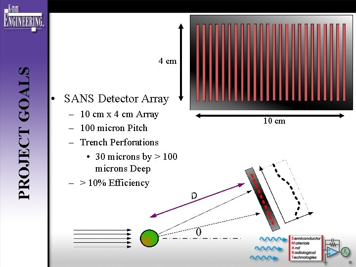
PROJECT GOALS 4 cm • SANS Detector Array – 10 cm x 4 cm Array – 100 micron Pitch – Trench Perforations • 30 microns by > 100 microns Deep – > 10% Efficiency 10 cm

Detector Design

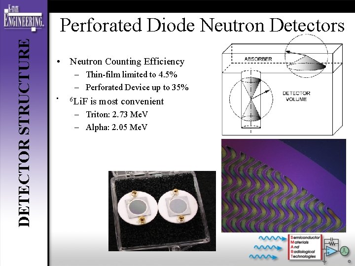
DETECTOR STRUCTURE Perforated Diode Neutron Detectors • Neutron Counting Efficiency – Thin-film limited to 4. 5% – Perforated Device up to 35% • 6 Li. F is most convenient – Triton: 2. 73 Me. V – Alpha: 2. 05 Me. V

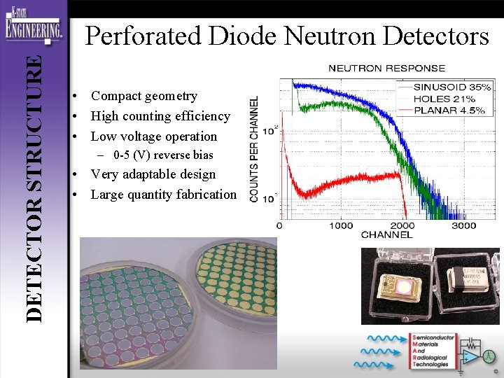
DETECTOR STRUCTURE Perforated Diode Neutron Detectors • Compact geometry • High counting efficiency • Low voltage operation – 0 -5 (V) reverse bias • Very adaptable design • Large quantity fabrication

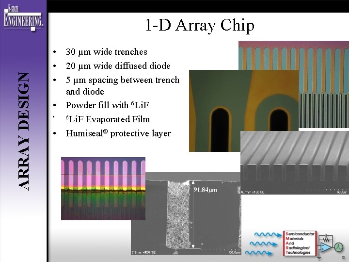
ARRAY DESIGN 1 -D Array Chip • 30 µm wide trenches • 20 µm wide diffused diode • 5 µm spacing between trench and diode • Powder fill with 6 Li. F • 6 Li. F Evaporated Film • Humiseal® protective layer

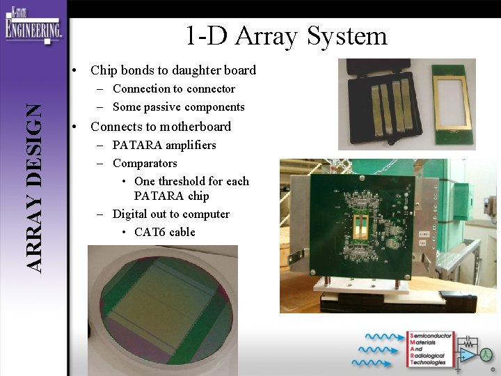
1 -D Array System ARRAY DESIGN • Chip bonds to daughter board – Connection to connector – Some passive components • Connects to motherboard – PATARA amplifiers – Comparators • One threshold for each PATARA chip – Digital out to computer • CAT 6 cable

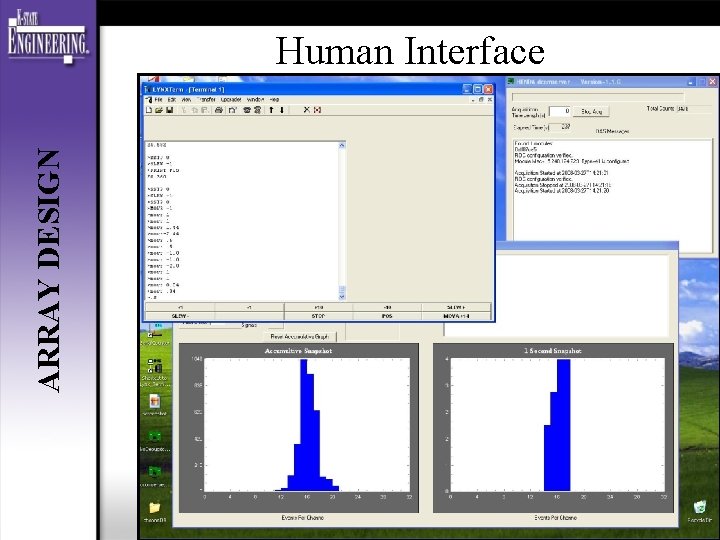
ARRAY DESIGN Human Interface

Performance

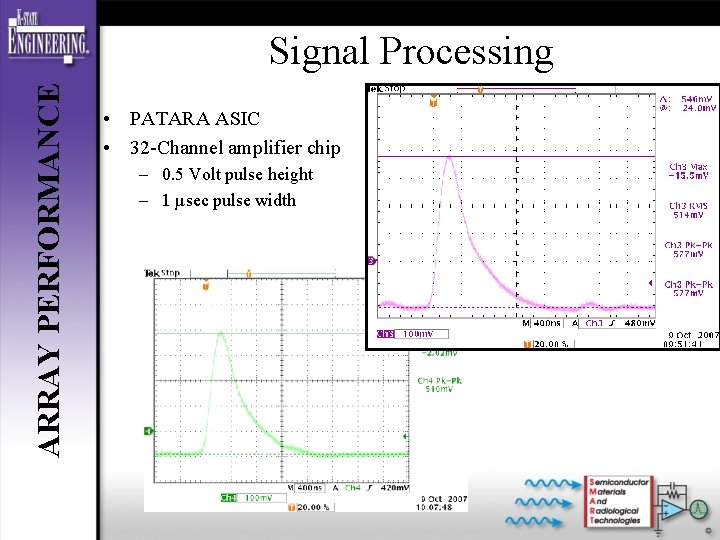
ARRAY PERFORMANCE Signal Processing • PATARA ASIC • 32 -Channel amplifier chip – 0. 5 Volt pulse height – 1 µsec pulse width

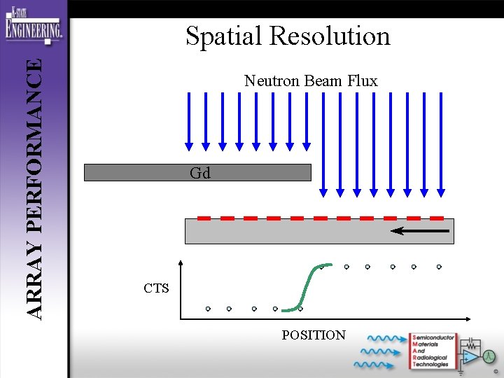
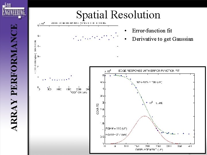
ARRAY PERFORMANCE Spatial Resolution Neutron Beam Flux Gd CTS POSITION

ARRAY PERFORMANCE Spatial Resolution • Error-function fit • Derivative to get Gaussian

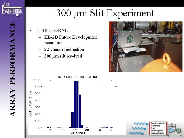
ARRAY PERFORMANCE 300 μm Slit Experiment • HFIR at ORNL – HB-2 D Future Development beam line – 32 -channel collection – 300 µm slit resolved

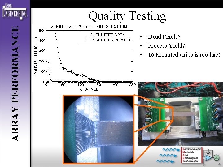
ARRAY PERFORMANCE Quality Testing • Dead Pixels? • Process Yield? • 16 Mounted chips is too late!

Conclusions • Successfully integrated system CONCLUSIONS – 106 count-rates should be possible • Excellent spatial resolution – 119 µm, FWHM • Efficiency exceeds thin-film detectors – 3 x, with room for improvement • Can test chips before assembly • Ready to assemble 1024 pixel array

Future Work

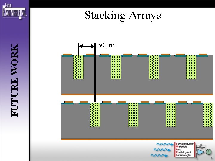
FUTURE WORK Stacking Arrays 60 µm

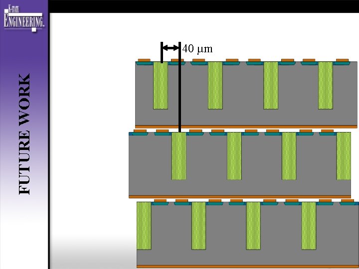
FUTURE WORK 40 µm

ACKNOWLEDGMENTS Ø Defense Threat Reduction Agency, contract DTRA-01 -03 C-0051 Ø National Science Foundation, IMR-MIP Grant, 2004 present Ø K-State Electronic Design Laboratory Ø Chuck Britton and University of Tennessee, Knoxville