1 Combinational Logic Design using SSI chips i

1
Combinational Logic Design using SSI chips i) Arithmetic Circuits ii) Code Convertor
Combinational Logic Circuits n n The term "combinational" comes to us from mathematics which means an unordered set where nobody cares which order the items came in With combinational logic, the circuit always produces the same output solely by a given set of inputs , regardless of the order the inputs are changed n If there are m outputs and n inputs then there are m Boolean functions, one describing each outputs n The inside of a combinational circuit is made of logic gates and it does not store any information (i. e. memoryless) n n There are circuits which depend on inputs and previous outputs. These circuits are called sequential logic where we will discuss in later chapter Combinational logic circuits are important components of digital systems 3
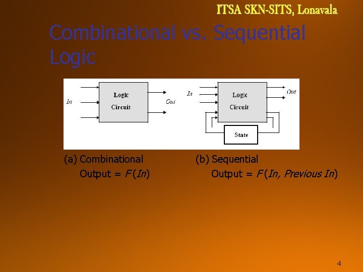
Combinational vs. Sequential Logic (a) Combinational Output = F (In) (b) Sequential Output = F (In, Previous In) 4
Designing Combinational Circuits n In general we have to do following steps: 1. 2. 3. 4. 5. From the specifications of the circuit, determine the required number of inputs and outputs and assign a letter symbol to each Derive the truth table that defines the relationship between inputs and outputs Obtain the simplified Boolean functions for each output as a function of the input variables Draw the logic diagram Verify the correctness of the design 5
Arithmetic Circuits n n Arithmetic circuits are the ones which perform arithmetic calculations on binary numbers like addition, subtraction, multiplication, and division etc. Arithmetic circuits can be built using logic circuits and they are excellent examples of combinational logic design n We will build arithmetic circuits by using the design procedure as stated previously 6
Adder n n Adders are the basic building blocks of all arithmetic circuits Adders add two binary numbers and give out sum and carry as output In modern computers adders reside in the arithmetic and logic unit (ALU) where other operations are performed Basically we have two types of adders n n Half Adder Full Adder 7
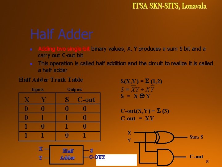
Half Adder n n Adding two single-bit binary values, X, Y produces a sum S bit and a carry out C-out bit This operation is called half addition and the circuit to realize it is called a half adder Half Adder Truth Table Inputs X 0 0 1 1 Y 0 1 X Y S(X, Y) = S (1, 2) Outputs S 0 1 1 0 Half Adder C-out 0 0 0 1 S C-OUT S = X Y C-out(X, Y) = S (3) C-out = XY X Y Sum S C-out 8
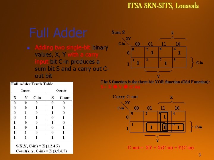
Full Adder n Sum S X XY Adding two single-bit binary values, X, Y with a carry input bit C-in produces a sum bit S and a carry out Cout bit 00 C-in 0 1 0 01 2 1 1 11 10 6 1 3 7 4 1 5 1 C-in Y The S function is the three-bit XOR function (Odd Function): S = X Y (C-in) Carry C-out X XY 00 C-in 0 1 01 0 2 1 3 11 6 7 1 10 4 5 1 C-in Y C-out = XY + X(C-in) + Y(C-in) 9
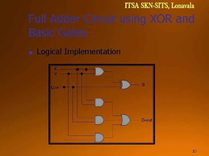
Full Adder Circuit using XOR and Basic Gates n Logical Implementation 10
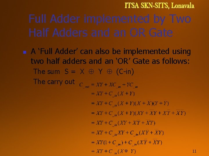
Full Adder implemented by Two Half Adders and an OR Gate n A ‘Full Adder’ can also be implemented using two half adders and an ‘OR’ Gate as follows: The sum S = X Y (C-in) The carry out 11
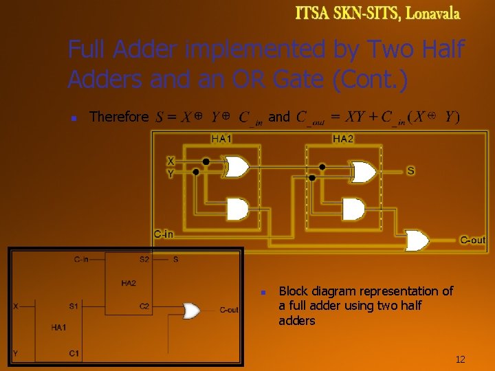
Full Adder implemented by Two Half Adders and an OR Gate (Cont. ) n Therefore and n Block diagram representation of a full adder using two half adders 12
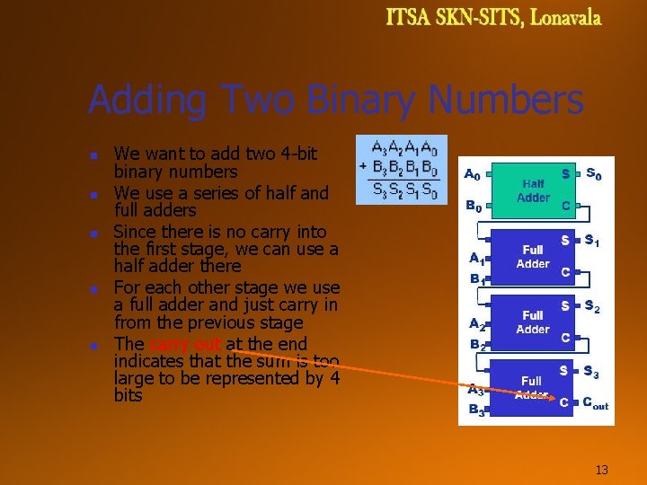
Adding Two Binary Numbers n n n We want to add two 4 -bit binary numbers We use a series of half and full adders Since there is no carry into the first stage, we can use a half adder there For each other stage we use a full adder and just carry in from the previous stage The carry out at the end indicates that the sum is too large to be represented by 4 bits 13

Subtraction n If we want to do subtraction, the circuit is very similar Looking at the truth table for A-B The only difference between a half adder and a half subtractor is the borrow n n n In order to perform this subtraction a digit has to be borrowed from the next highest column of the subtraction When it borrows, it gets a 2 and the operation then becomes 2 - 1 =1 The Borrow output is set to indicate that borrow operation is required 14
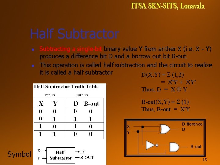
Half Subtractor n n Subtracting a single-bit binary value Y from anther X (i. e. X - Y) produces a difference bit D and a borrow out bit B-out This operation is called half subtraction and the circuit to realize it is called a half subtractor D(X, Y) = (1, 2) = X'Y + XY' Thus, D = X Y B-out(X, Y) = (1) Thus, B-out = X'Y Symbol 15
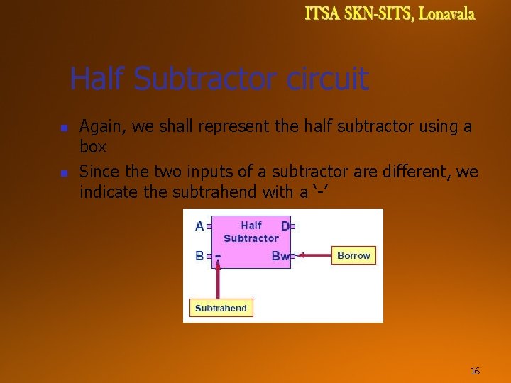
Half Subtractor circuit n n Again, we shall represent the half subtractor using a box Since the two inputs of a subtractor are different, we indicate the subtrahend with a ‘-’ 16
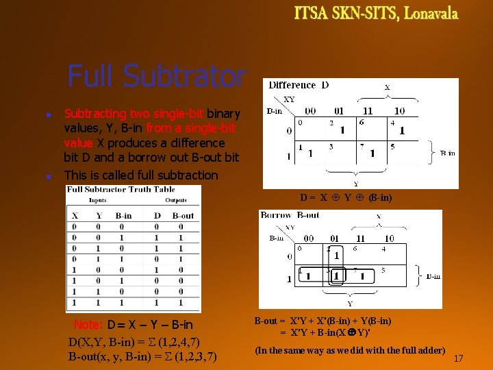
Full Subtrator n n Subtracting two single-bit binary values, Y, B-in from a single-bit value X produces a difference bit D and a borrow out B-out bit This is called full subtraction D = X Y (B-in) Note: D= X – Y – B-in D(X, Y, B-in) = (1, 2, 4, 7) B-out(x, y, B-in) = (1, 2, 3, 7) B-out = X'Y + X'(B-in) + Y(B-in) = X'Y + B-in(X Y)' (In the same way as we did with the full adder) 17
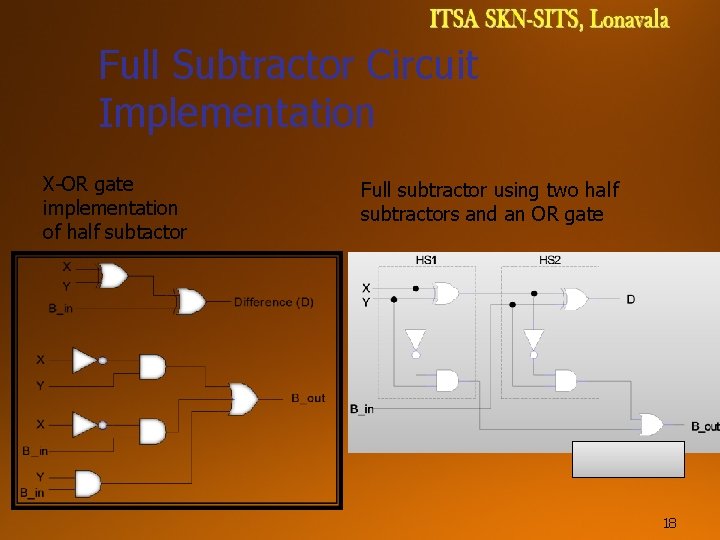
Full Subtractor Circuit Implementation X-OR gate implementation of half subtactor Full subtractor using two half subtractors and an OR gate 18
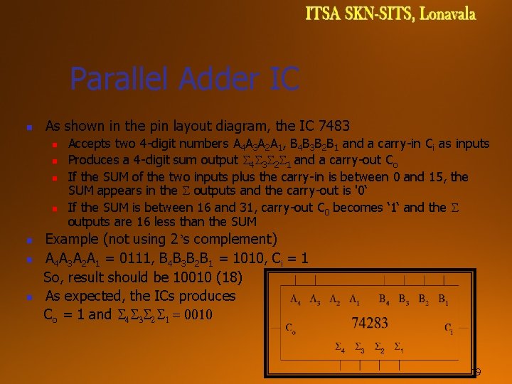
Parallel Adder IC n As shown in the pin layout diagram, the IC 7483 n n n n Accepts two 4 -digit numbers A 4 A 3 A 2 A 1, B 4 B 3 B 2 B 1 and a carry-in Ci as inputs Produces a 4 -digit sum output 4 3 2 1 and a carry-out Co If the SUM of the two inputs plus the carry-in is between 0 and 15, the SUM appears in the outputs and the carry-out is '0‘ If the SUM is between 16 and 31, carry-out C 0 becomes ‘ 1‘ and the outputs are 16 less than the SUM Example (not using 2’s complement) A 4 A 3 A 2 A 1 = 0111, B 4 B 3 B 2 B 1 = 1010, Ci = 1 So, result should be 10010 (18) As expected, the ICs produces Co = 1 and 19
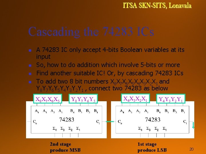
Cascading the 74283 ICs n n A 74283 IC only accept 4 -bits Boolean variables at its input So, how to do addition which involve 5 -bits or more Find another suitable IC! Or, by cascading 74283 ICs To add two 8 bit numbers X 8 X 7 X 6 X 5 X 4 X 3 X 2 X 1 and Y 8 Y 7 Y 6 Y 5 Y 4 Y 3 Y 2 Y 1 , connect two 74283 as below X 8 X 7 X 6 X 5 Y 8 Y 7 Y 6 Y 5 2 nd stage produce MSB X 4 X 3 X 2 X 1 Y 4 Y 3 Y 2 Y 1 1 st stage produce LSB 20
n-bit Subtractors n An n-bit subtracor used to subtract an n-bit number Y from another n-bit number X (i. e. X - Y) can be built by using an n-bit adder and n inverters: 1. 2. n Find two’s complement (1's complement plus 1) of Y by: Inverting all the bits of Y using the n inverters Adding 1 by setting the carry in of the least significant position to 1 The original subtraction (X - Y) now becomes an addition of X to two’s complement of Y using the nbit adder 21
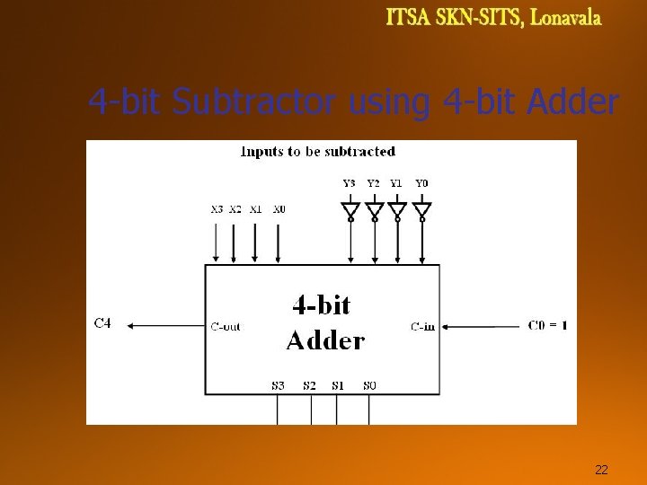
4 -bit Subtractor using 4 -bit Adder 22
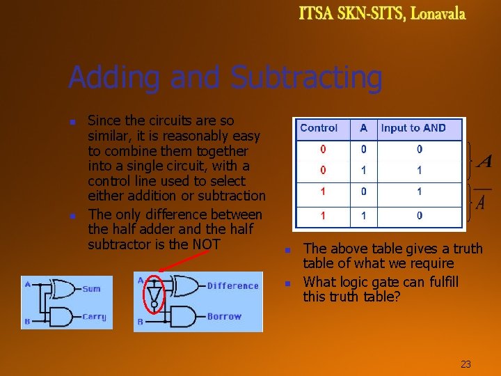
Adding and Subtracting n n Since the circuits are so similar, it is reasonably easy to combine them together into a single circuit, with a control line used to select either addition or subtraction The only difference between the half adder and the half subtractor is the NOT n n The above table gives a truth table of what we require What logic gate can fulfill this truth table? 23
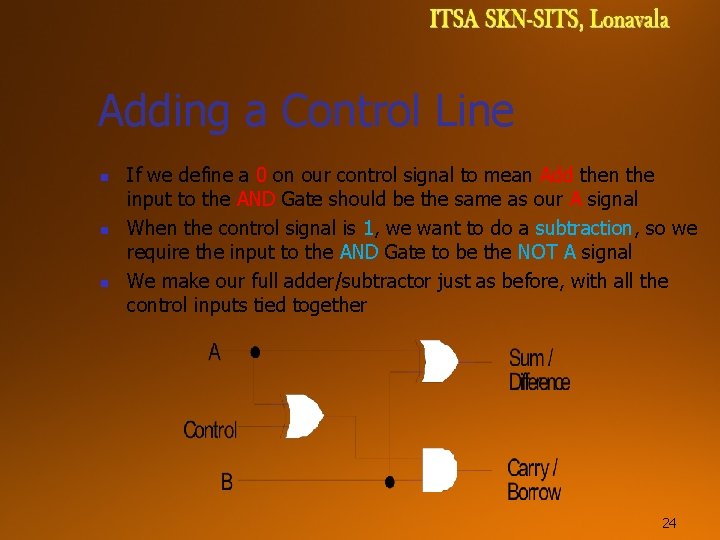
Adding a Control Line n n n If we define a 0 on our control signal to mean Add then the input to the AND Gate should be the same as our A signal When the control signal is 1, we want to do a subtraction, so we require the input to the AND Gate to be the NOT A signal We make our full adder/subtractor just as before, with all the control inputs tied together 24
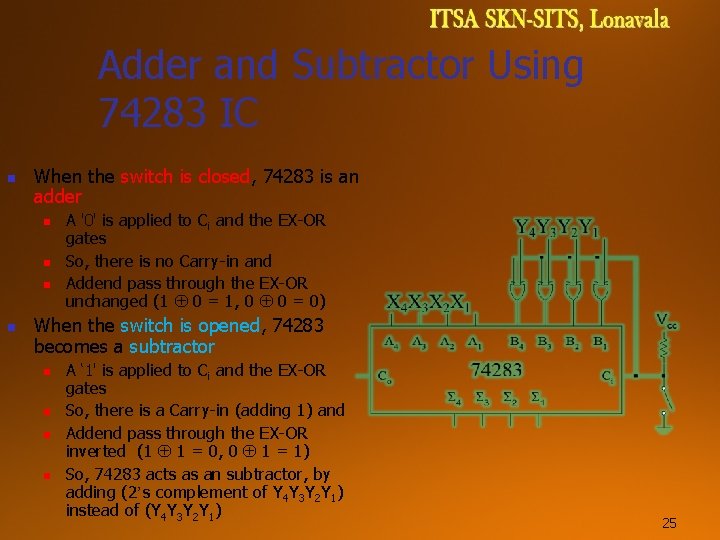
Adder and Subtractor Using 74283 IC n When the switch is closed, 74283 is an adder n n A '0' is applied to Ci and the EX-OR gates So, there is no Carry-in and Addend pass through the EX-OR unchanged (1 0 = 1, 0 0 = 0) When the switch is opened, 74283 becomes a subtractor n n A ‘ 1' is applied to Ci and the EX-OR gates So, there is a Carry-in (adding 1) and Addend pass through the EX-OR inverted (1 1 = 0, 0 1 = 1) So, 74283 acts as an subtractor, by adding (2’s complement of Y 4 Y 3 Y 2 Y 1) instead of (Y 4 Y 3 Y 2 Y 1) 25
BCD Adder n n n When the sum of two digits is less than or equal to 9 then the ordinary 4 -bit adder can be used But if the sum of two digits is greater than 9 then a correction must be added “I. e adding 0110” We need to design a circuit that is capable of doing the correct addition

Examples : 1. CASE I : Sum <= 9 & carry = 0. n Add BCD digits 3 & 4 1. 0011 +0100 ----0111 Answer is valid BCD number = (7)BCD & so addition of 0110 is not added.
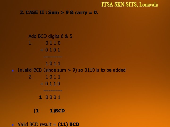
2. CASE II : Sum > 9 & carry = 0. n Add BCD digits 6 & 5 1. 0110 +0101 -----1011 Invalid BCD (since sum > 9) so 0110 is to be added 2. 1011 +0110 -----1 0001 (1 n 1)BCD Valid BCD result = (11) BCD
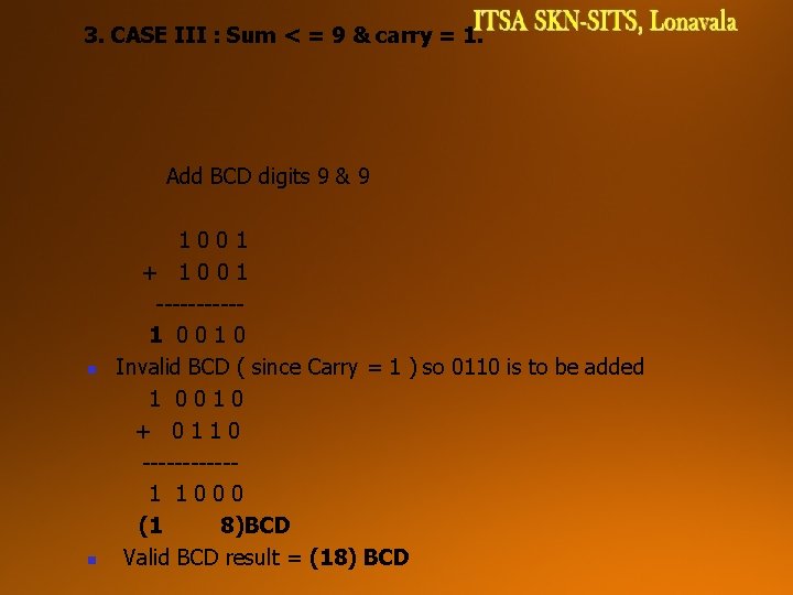
3. CASE III : Sum < = 9 & carry = 1. Add BCD digits 9 & 9 n n 1001 + 1001 -----1 0010 Invalid BCD ( since Carry = 1 ) so 0110 is to be added 1 0010 + 0110 ------1 1000 (1 8)BCD Valid BCD result = (18) BCD
Design of BCD Adder n n n Design of BCD adder : To execute first step i. e. binary addition of two 4 bit numbers we will use IC 7483 ( with Cin = 0 ), which is 4 bit binary adder. We need to design a digital circuit which will sense sum & carry of IC 7483 & if sum exceeds 9 or carry = 1, this digital circuit will produce high output otherwise its output will be zero. 30
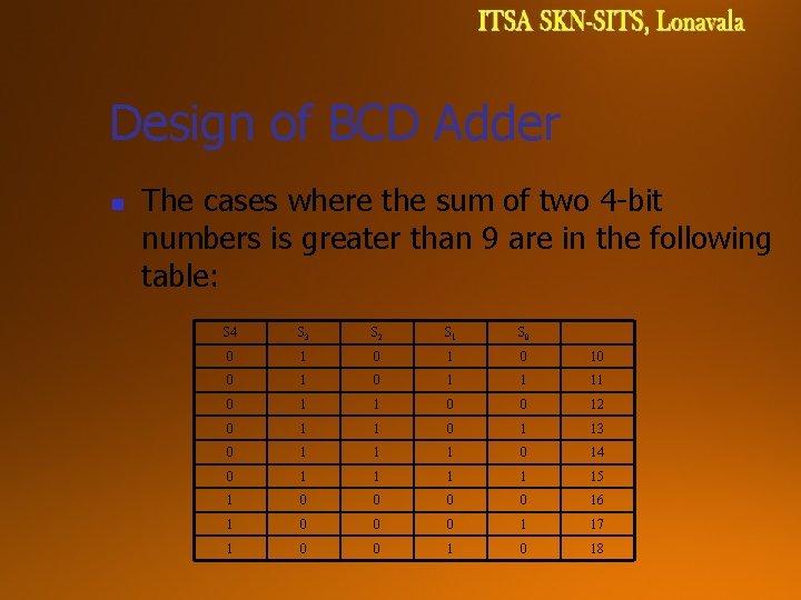
Design of BCD Adder n The cases where the sum of two 4 -bit numbers is greater than 9 are in the following table: S 4 S 3 S 2 S 1 S 0 0 1 0 10 0 1 1 11 0 1 1 0 0 12 0 1 13 0 1 1 1 0 14 0 1 1 15 1 0 0 16 1 0 0 0 1 17 1 0 0 18
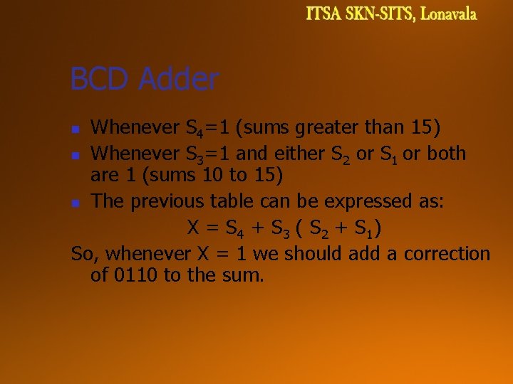
BCD Adder Whenever S 4=1 (sums greater than 15) n Whenever S 3=1 and either S 2 or S 1 or both are 1 (sums 10 to 15) n The previous table can be expressed as: X = S 4 + S 3 ( S 2 + S 1) So, whenever X = 1 we should add a correction of 0110 to the sum. n
![Inputs: [A]=0101, [B]= 0011, Co=0 0011 0101 0 0 0 0 0 1000 1 Inputs: [A]=0101, [B]= 0011, Co=0 0011 0101 0 0 0 0 0 1000 1](http://slidetodoc.com/presentation_image_h2/c1e31bca1428616cdf8e5d983c903434/image-33.jpg)
Inputs: [A]=0101, [B]= 0011, Co=0 0011 0101 0 0 0 0 0 1000 1 1 0 0000
![Inputs: [A]=0111, [B]= 0110, Co=0 0111 0 1 1 1 1101 1 0 0 Inputs: [A]=0111, [B]= 0110, Co=0 0111 0 1 1 1 1101 1 0 0](http://slidetodoc.com/presentation_image_h2/c1e31bca1428616cdf8e5d983c903434/image-34.jpg)
Inputs: [A]=0111, [B]= 0110, Co=0 0111 0 1 1 1 1101 1 0 0 1 1 0110
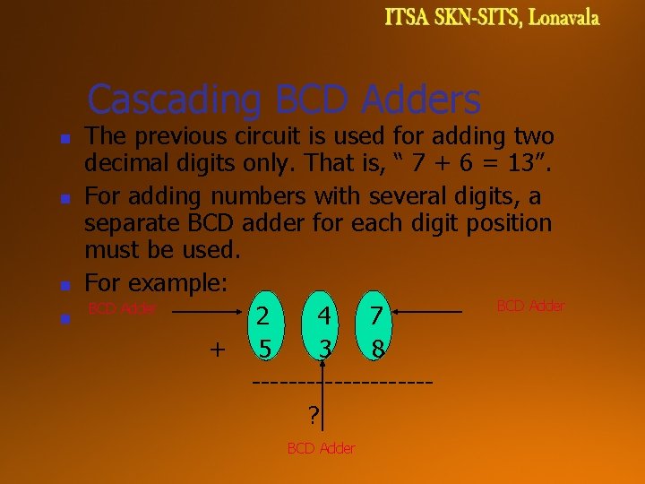
Cascading BCD Adders n n The previous circuit is used for adding two decimal digits only. That is, “ 7 + 6 = 13”. For adding numbers with several digits, a separate BCD adder for each digit position must be used. For example: BCD Adder 2 4 7 + 5 3 8 ----------? BCD Adder
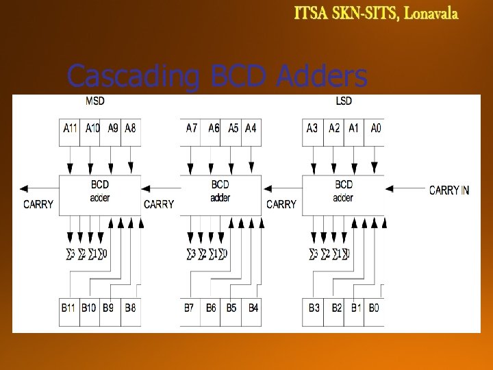
Cascading BCD Adders
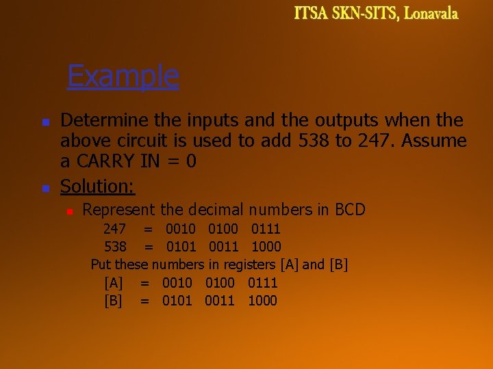
Example n n Determine the inputs and the outputs when the above circuit is used to add 538 to 247. Assume a CARRY IN = 0 Solution: n Represent the decimal numbers in BCD 247 = 0010 0100 0111 538 = 0101 0011 1000 Put these numbers in registers [A] and [B] [A] = 0010 0100 0111 [B] = 0101 0011 1000
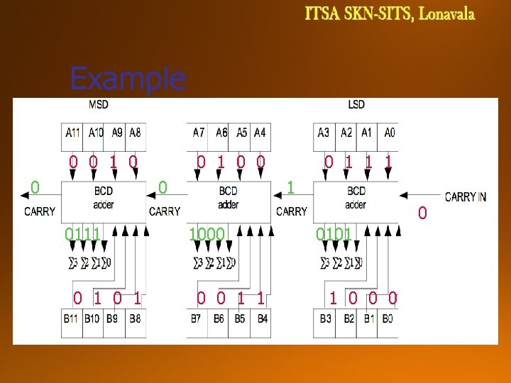
Example 0 0 1 0 0 0 0 1 1 0 0111 0 1 1000 0 0 1 1 0101 1 0 0 0
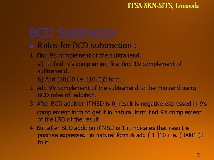
BCD Subtractor n Rules for BCD subtraction : 1. Find 9’s complement of the subtrahend. a) To find 9’s complement first find 1’s complement of subtrahend. b) Add (10)10 i. e. (1010)2 to it. 2. Add 9’s complement of the subtrahend to the minuend using BCD rules of addition. 3. After BCD addition if MSD is 0, result is negative expressed in 9’s complement form to get it in natural form find 9’s complement of the LSD of the result. 4. But after BCD addition if MSD is 1 it indicates that result is positive expressed in natural form & add ( 1 )10 i. e. ( 0001 )2 to it. 39
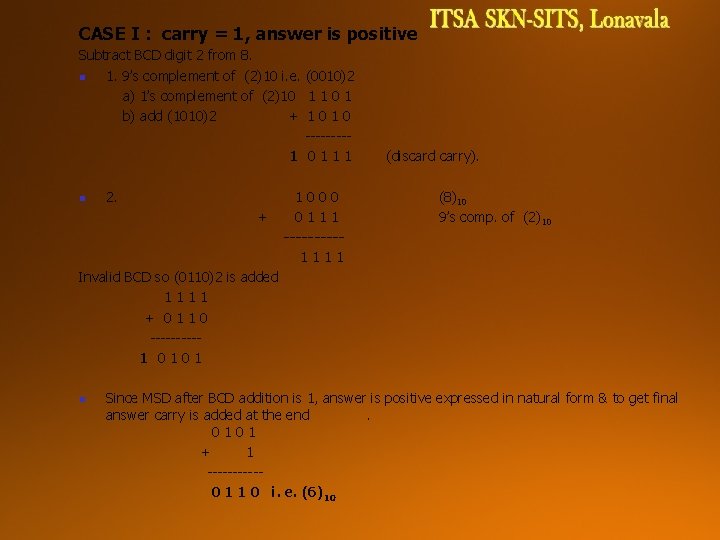
CASE I : carry = 1, answer is positive Subtract BCD digit 2 from 8. n 1. 9’s complement of (2)10 i. e. (0010)2 a) 1’s complement of (2)10 1 1 0 1 b) add (1010)2 + 1010 ----1 0111 n 2. + 1000 0111 -----1111 (discard carry). (8)10 9’s comp. of (2)10 Invalid BCD so (0110)2 is added 1111 + 0110 -----1 0101 n Since MSD after BCD addition is 1, answer is positive expressed in natural form & to get final answer carry is added at the end. 0101 + 1 -----0 1 1 0 i. e. (6)10
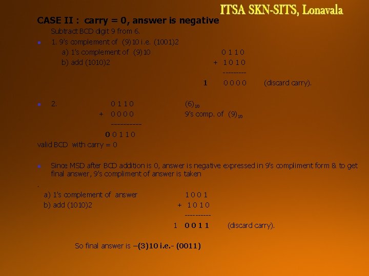
CASE II : carry = 0, answer is negative n Subtract BCD digit 9 from 6. 1. 9’s complement of (9)10 i. e. (1001)2 a) 1’s complement of (9)10 b) add (1010)2 0110 + 0000 -----00110 valid BCD with carry = 0 n n 2. 0110 + 1010 ----1 0000 (discard carry). (6)10 9’s comp. of (9)10 Since MSD after BCD addition is 0, answer is negative expressed in 9’s compliment form & to get final answer, 9’s compliment of answer is taken . a) 1’s complement of answer b) add (1010)2 1001 + 1010 -----1 0011 So final answer is –(3)10 i. e. - (0011) (discard carry).
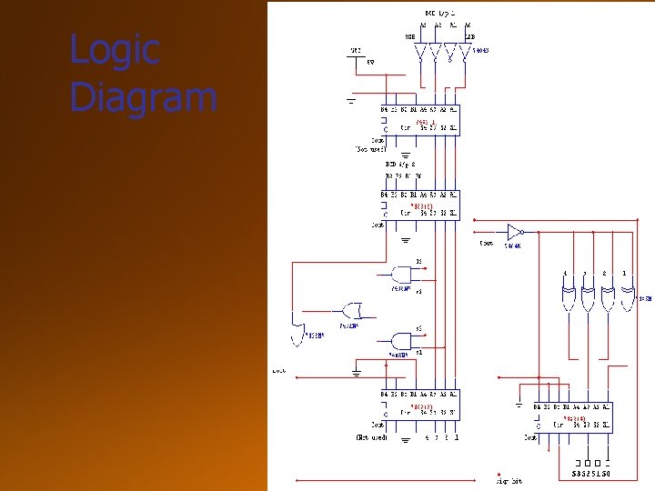
Design of BCD Subtractor 1. To execute first step i. e. to find 9’s compliment of subtrahend a) First we find 1 s compliment of subtrahend. b) Then add (10)10 i. e. (1010)2 to 1’s compliment of subtrahend. We use inverter to get 1’s compliment of subtrahend since subtrahend is 4 bit we need 4 inverters and to add this to (1010)2, 4 bit binary adder IC 7483 is used. n 2. Circuit for BCD addition of 9’s compliment of subtrahend and minuend we will use already designed BCD adder n 3. Circuit to get answer in correct form. If MSD after BCD addition is 0, answer is negative expressed in 9’s compliment form & to get answer in correct form we have to find 9’s compliment of the result. If MSD after BCD addition is 1, answer is positive expressed in natural form & to get final answer carry is added to the earlier answer. n
Logic Diagram
CIRCUIT DELAYS (1/5) n Given a logic gate with delay t. If inputs are stable at times t 1, t 2, …, tn, then the earliest time in which the output will be stable is: max( t 1, t 2, …, tn ) + t t 1 t 2 : tn n : Logic Gate max (t 1, t 2, . . . , tn ) + t To calculate the delays of all outputs of a combinational circuit, repeat above rule for all gates.
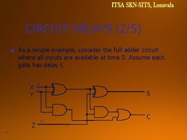
CIRCUIT DELAYS (2/5) n As a simple example, consider the full adder circuit where all inputs are available at time 0. Assume each gate has delay t. X Y Z 0 0 S 0 C
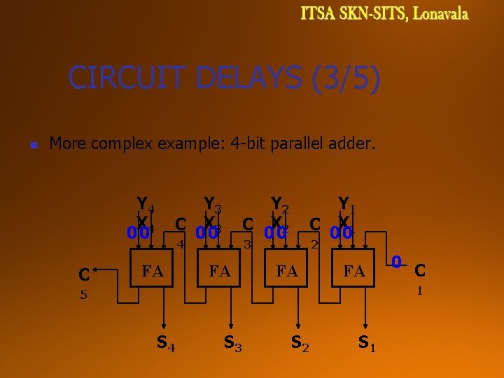
CIRCUIT DELAYS (3/5) n More complex example: 4 -bit parallel adder. Y 4 X 4 00 C Y 3 C X 3 00 Y 2 C X 2 00 4 FA Y 1 C X 1 00 3 FA 2 FA FA 0 C 1 5 S 4 S 3 S 2 S 1

CIRCUIT DELAYS (4/5) n n Analyse the delay for the repeated block. Xi where Xi, Yi are 0 Si stable at 0 t, while Full Yi 0 Ci is assumed to be Adder C i+1 Ci mt stable at mt. Performing the delay calculation: Xi Yi 0 0 max(0, 0)+t = t t Ci mt max(t, mt)+t Si max(t, mt)+2 t Ci+1
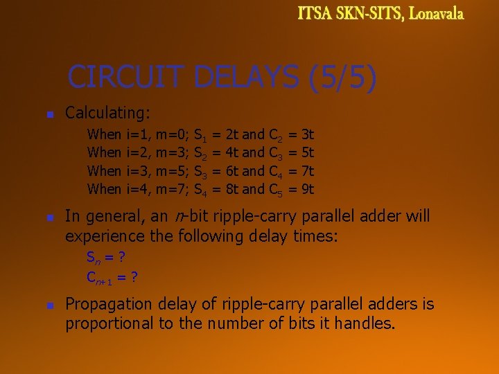
CIRCUIT DELAYS (5/5) n Calculating: When n i=1, i=2, i=3, i=4, m=0; m=3; m=5; m=7; S 1 S 2 S 3 S 4 = = 2 t 4 t 6 t 8 t and and C 2 C 3 C 4 C 5 = = 3 t 5 t 7 t 9 t In general, an n-bit ripple-carry parallel adder will experience the following delay times: Sn = ? Cn+1 = ? n Propagation delay of ripple-carry parallel adders is proportional to the number of bits it handles.
FASTER CIRCUITS n Three ways of improving the speed of circuits: n Use better technology (eg. ECL faster than TTL gates) BUT n n n Use gate-level designs to two-level circuits! (use sumof-products/product-of-sums) BUT n n n Faster technology is more expensive, needs more power, lower-level of integrations Physical limits (eg. speed of light, size of atom) Complicated designs for large circuits Product/sum terms need MANY inputs! Use clever look-ahead techniques BUT n There additional costs (hopefully reasonable).
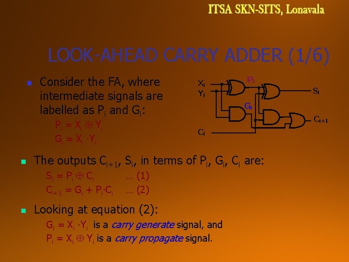
LOOK-AHEAD CARRY ADDER (1/6) n Consider the FA, where intermediate signals are labelled as Pi and Gi: Pi = X i Y i Gi = Xi ∙Yi n Pi Si Gi Ci+1 Ci The outputs Ci+1, Si, in terms of Pi, Gi, Ci are: Si = P i C i Ci+1 = Gi + Pi∙Ci n Xi Yi … (1) … (2) Looking at equation (2): Gi = Xi ∙Yi is a carry generate signal, and Pi = Xi Yi is a carry propagate signal.
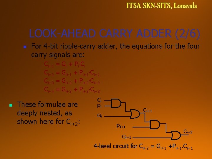
LOOK-AHEAD CARRY ADDER (2/6) n For 4 -bit ripple-carry adder, the equations for the four carry signals are: Ci+1 Ci+2 Ci+3 Ci+4 n = = Gi + Pi∙Ci Gi+1 + Pi+1∙Ci+1 Gi+2 + Pi+2∙Ci+2 Gi+3 + Pi+3∙Ci+3 These formulae are deeply nested, as shown here for Ci+2: Ci Pi Ci+1 Gi Pi+1 Gi+1 Ci+2 4 -level circuit for Ci+2 = Gi+1 +Pi+1. Ci+1
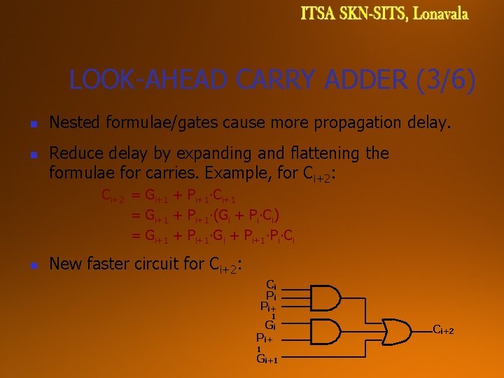
LOOK-AHEAD CARRY ADDER (3/6) n n Nested formulae/gates cause more propagation delay. Reduce delay by expanding and flattening the formulae for carries. Example, for Ci+2: Ci+2 = Gi+1 + Pi+1∙Ci+1 = Gi+1 + Pi+1∙(Gi + Pi∙Ci) = Gi+1 + Pi+1∙Gi + Pi+1∙Pi∙Ci n New faster circuit for Ci+2: Ci Pi Pi+ 1 Gi+1 Ci+2
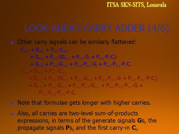
LOOK-AHEAD CARRY ADDER (4/6) n Other carry signals can be similarly flattened: Ci+3 = Gi+2 + Pi+2∙Ci+2 = Gi+2 + Pi+2∙(Gi+1 + Pi+1∙Gi + Pi+1∙Pi∙Ci) = Gi+2 + Pi+2∙Gi+1 + Pi+2∙Pi+1∙Gi + Pi+2∙Pi+1∙Pi∙Ci Ci+4= Gi+3 + Pi+3∙Ci+3 = Gi+3 + Pi+3∙(Gi+2 + Pi+2∙Gi+1 + Pi+2∙Pi+1∙Gi + Pi+2∙Pi+1∙Pi∙Ci) = Gi+3 + Pi+3∙Gi+2 + Pi+3∙Pi+2∙Gi+1 + Pi+3∙Pi+2∙Pi+1∙Gi + Pi+3∙Pi+2∙Pi+1∙Pi∙Ci n n Note that formulae gets longer with higher carries. Also, all carries are two-level sum-of-products expressions, in terms of the generate signals Gs, the propagate signals Ps, and the first carry-in Ci.
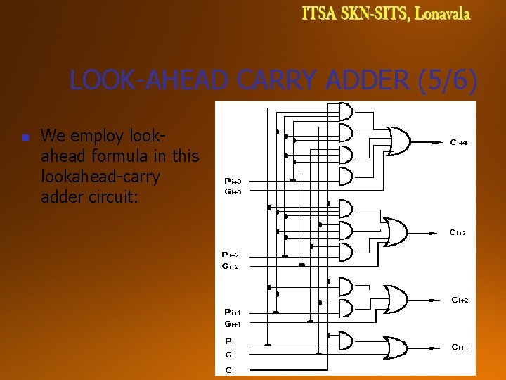
LOOK-AHEAD CARRY ADDER (5/6) n We employ lookahead formula in this lookahead-carry adder circuit:
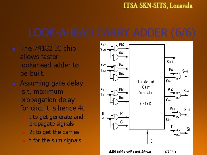
LOOK-AHEAD CARRY ADDER (6/6) n n The 74182 IC chip allows faster lookahead adder to be built. Assuming gate delay is t, maximum propagation delay for circuit is hence 4 t n n n t to get generate and propagate signals 2 t to get the carries t for the sum signals
Code Converter Binary to Gray Code Gray to Binary Code BCD to Excess – 3 Code Excess-3 to BCD Code
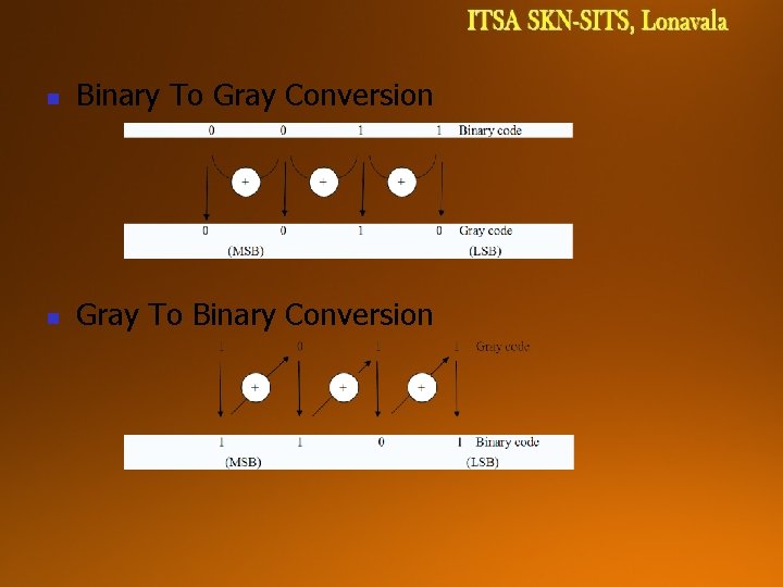
n Binary To Gray Conversion n Gray To Binary Conversion
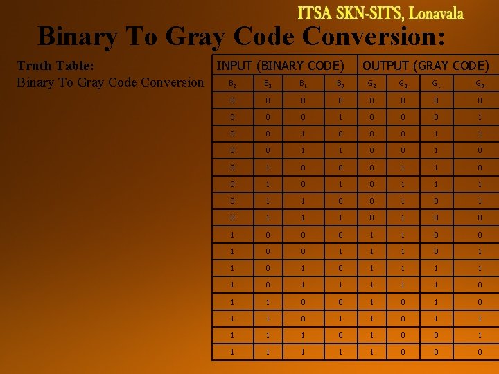
Binary To Gray Code Conversion: INPUT (BINARY CODE) Truth Table: B B Binary To Gray Code Conversion 3 2 1 0 OUTPUT (GRAY CODE) G 3 G 2 G 1 G 0 0 0 1 0 0 0 1 1 0 0 0 1 1 0 0 1 0 1 0 1 1 1 0 1 0 0 0 1 1 1 0 1 0 1 1 1 1 1 0 0 1 0 1 1 1 0 0 1 1 1 0 0 0
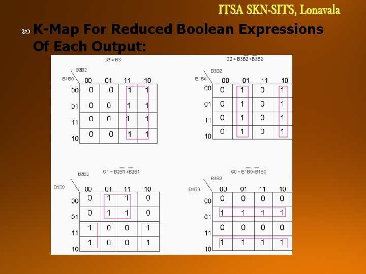
K-Map For Reduced Boolean Expressions Of Each Output:
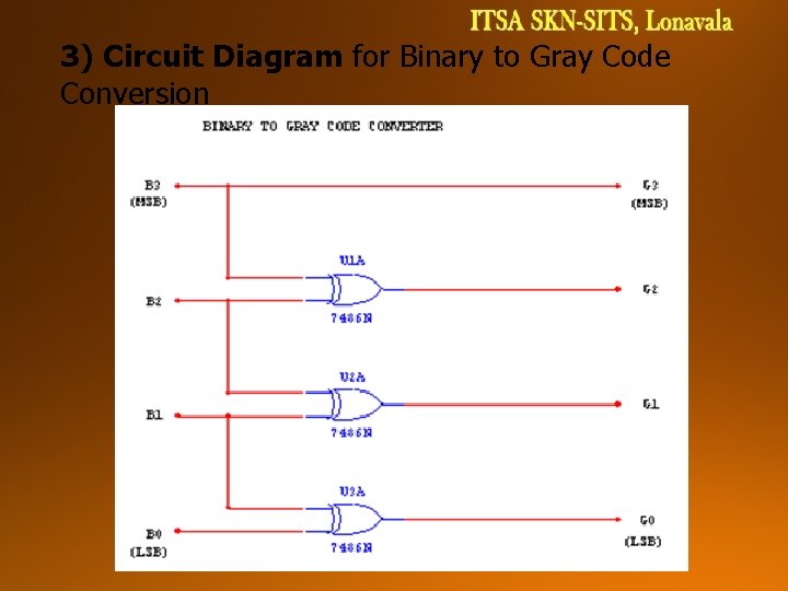
3) Circuit Diagram for Binary to Gray Code Conversion
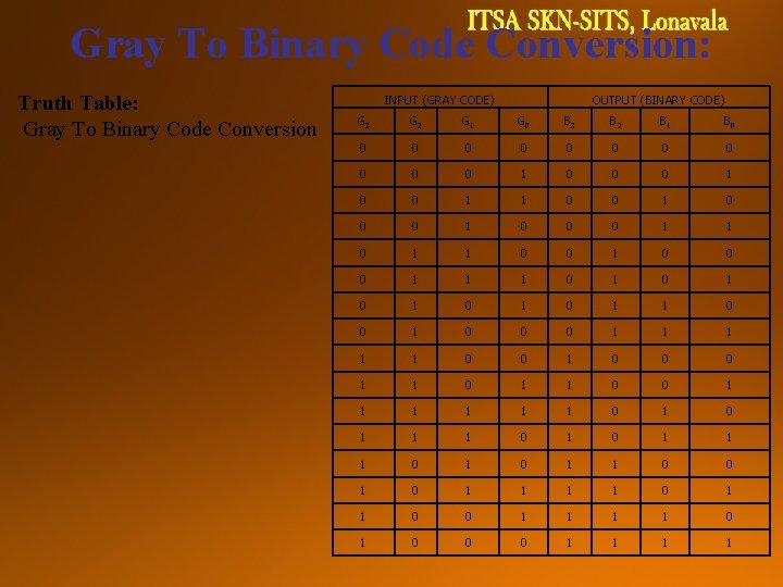
Gray To Binary Code Conversion: Truth Table: Gray To Binary Code Conversion INPUT (GRAY CODE) OUTPUT (BINARY CODE) G 3 G 2 G 1 G 0 B 3 B 2 B 1 B 0 0 0 1 0 0 0 1 0 0 0 1 1 0 0 0 1 1 1 0 1 0 1 0 1 1 0 0 0 1 1 0 0 1 1 1 0 1 1 0 0 1 1 1 1 0 0 1 1 0 1 0 0 0 1 1
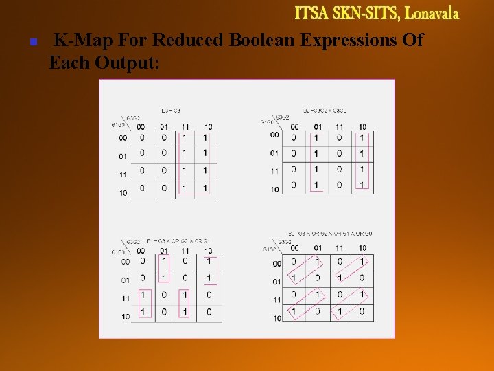
n K-Map For Reduced Boolean Expressions Of Each Output:
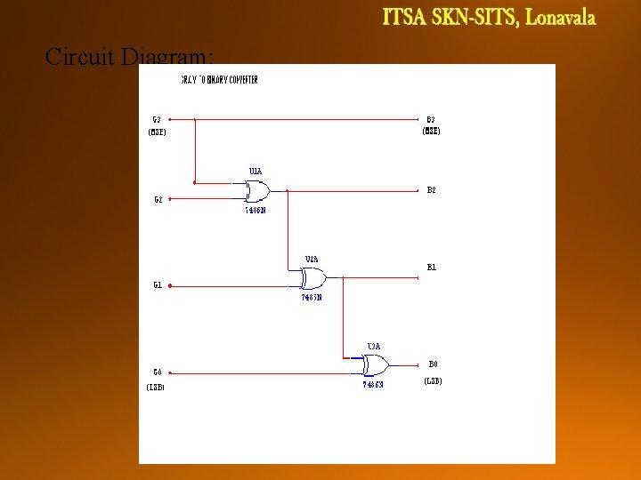
Circuit Diagram:
- Slides: 63