
1 BIPOLAR JUNCTION TRANSISTORS BJTs 20052021 CHAPTER 4
1 BIPOLAR JUNCTION TRANSISTORS (BJTs) 20/05/2021 CHAPTER 4
INTRODUCTION 20/05/2021 �What is transistor? � three-terminal device whose output current, voltage and/or power are controlled by its input. � 2 basic transistor types: BJT and FET 2
OBJECTIVES Describe the basic structure of the bipolar junction transistor (BJT) Explain and analyze basic transistor bias and operation Discuss the parameters and characteristics of a transistor and how they apply to transistor circuits 20/05/2021 3
LECTURE OUTLINE 2. 3. 4. 5. 6. 20/05/2021 1. BJT structure Basic BJT operations BJT Characteristics and Parameters BJT as an amplifier BJT as a switch Summary 4
20/05/2021 1. BJT STRUCTURE 5
1. BJT STRUCTURE 20/05/2021 6
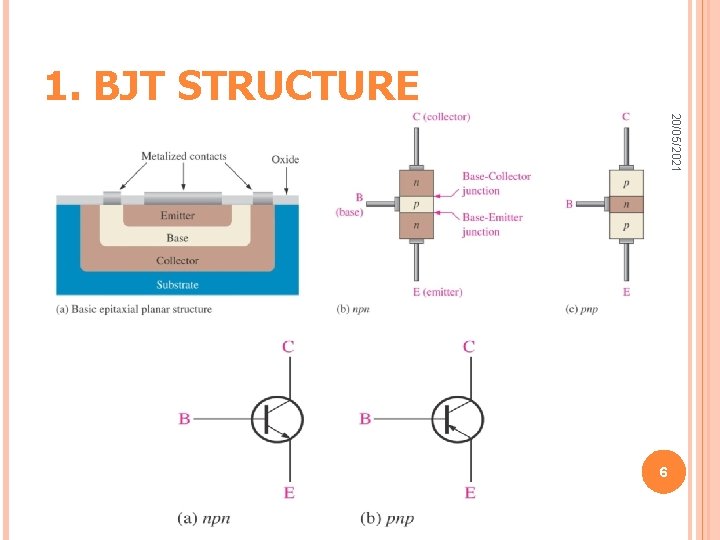
1. BJT STRUCTURE BJT constructed with three doped semiconductor regions The region are called emitter (E), base (B) and collector (C) The BJT have 2 types: 20/05/2021 1. Two n region separate by a p region 2. Two p region separated by a n region pn junction joining the base region and the emitter regionbase-emiter junction pn junction joining the base region and the collector region-base-collector junction base region is lightly doped and very thin compared to the heavily doped emitter and the moderately doped collector region 7
1. BJT STRUCTURE 20/05/2021 BJT schematic symbol The arrow on schematic symbol is important because: � Identify the component terminal § arrow is always drawn on the emitter terminal. § terminal opposite emitter is collector and the center terminal is base. � The arrow always points toward n-type material § arrow point toward base, transistor is pnp type. § points toward emitter, transistor is npn type. 8
20/05/2021 2. BJT OPERATION 9
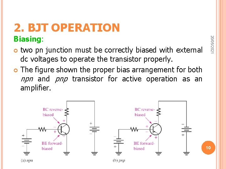
2. BJT OPERATION 20/05/2021 Biasing: two pn junction must be correctly biased with external dc voltages to operate the transistor properly. The figure shown the proper bias arrangement for both npn and pnp transistor for active operation as an amplifier. 10
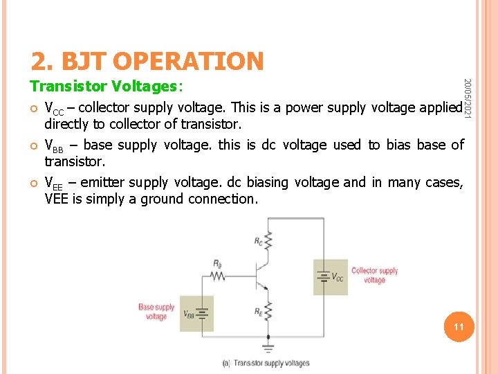
2. BJT OPERATION 20/05/2021 Transistor Voltages: VCC – collector supply voltage. This is a power supply voltage applied directly to collector of transistor. VBB – base supply voltage. this is dc voltage used to bias base of transistor. VEE – emitter supply voltage. dc biasing voltage and in many cases, VEE is simply a ground connection. 11

2. BJT OPERATION 20/05/2021 Transistor Voltages: VC – dc voltage measured from collector terminal of component to ground VB – dc voltage measured from base terminal to ground. VE – dc voltage measured from emitter terminal to ground. 12
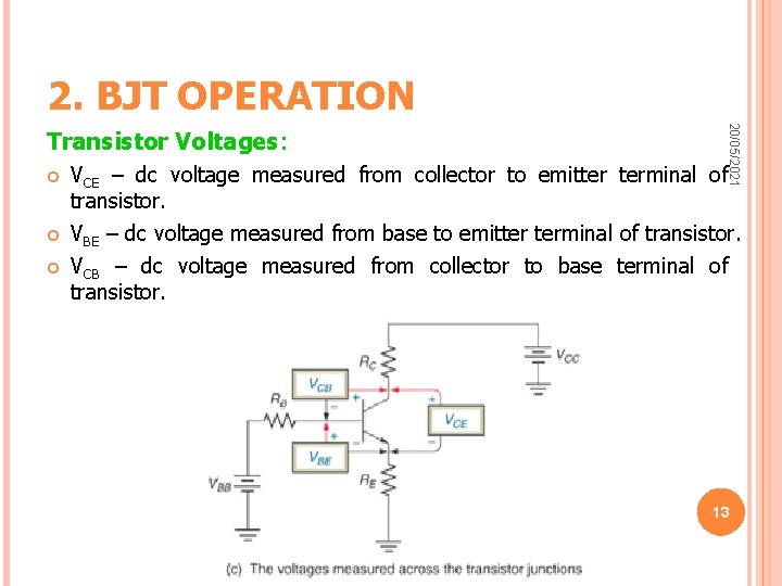
2. BJT OPERATION 20/05/2021 Transistor Voltages: VCE – dc voltage measured from collector to emitter terminal of transistor. VBE – dc voltage measured from base to emitter terminal of transistor. VCB – dc voltage measured from collector to base terminal of transistor. 13
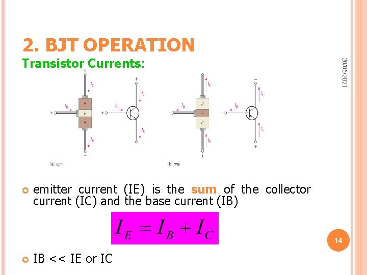
2. BJT OPERATION 20/05/2021 Transistor Currents: emitter current (IE) is the sum of the collector current (IC) and the base current (IB) 14 IB << IE or IC
20/05/2021 3. BJT CHARACTERISTICS & PARAMETERS 15
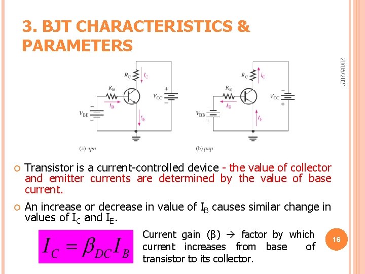
3. BJT CHARACTERISTICS & PARAMETERS 20/05/2021 Transistor is a current-controlled device - the value of collector and emitter currents are determined by the value of base current. An increase or decrease in value of IB causes similar change in values of IC and IE. Current gain (β) factor by which current increases from base of transistor to its collector. 16
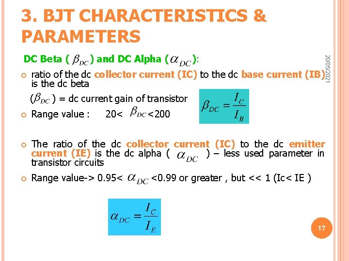
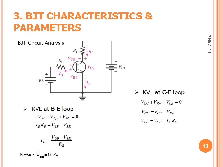
3. BJT CHARACTERISTICS & PARAMETERS ) and DC Alpha ( ): 20/05/2021 DC Beta ( ratio of the dc collector current (IC) to the dc base current (IB) is the dc beta ( ) = dc current gain of transistor Range value : 20< <200 The ratio of the dc collector current (IC) to the dc emitter current (IE) is the dc alpha ( ) – less used parameter in transistor circuits Range value-> 0. 95< <0. 99 or greater , but << 1 (Ic< IE ) 17
3. BJT CHARACTERISTICS & PARAMETERS 20/05/2021 18
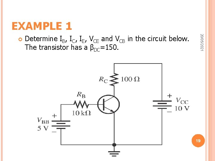
EXAMPLE 1 Determine IB, IC, IE, VCE and VCB in the circuit below. The transistor has a βDC=150. 20/05/2021 19
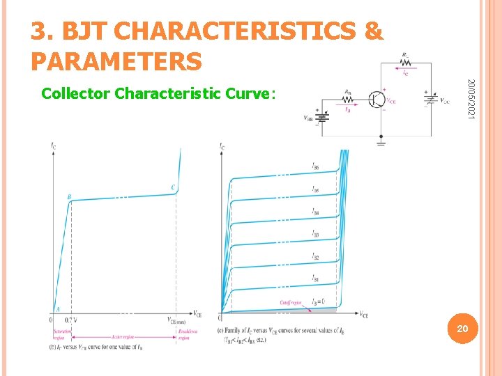
3. BJT CHARACTERISTICS & PARAMETERS 20/05/2021 Collector Characteristic Curve: 20
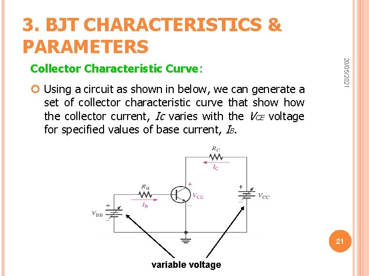
3. BJT CHARACTERISTICS & PARAMETERS Using a circuit as shown in below, we can generate a set of collector characteristic curve that show the collector current, Ic varies with the VCE voltage for specified values of base current, IB. 20/05/2021 Collector Characteristic Curve: 21 variable voltage

3. BJT CHARACTERISTICS & PARAMETERS 20/05/2021 Cutoff region Both transistor junctions are reverse biased. With large depletion region between C-B and E-B, reverse current, ICEO passes from emitter to collector and can be neglected. So, VCE = VCC 22
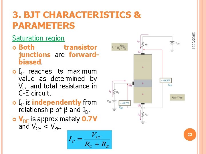
3. BJT CHARACTERISTICS & PARAMETERS 20/05/2021 Saturation region Both transistor junctions are forwardbiased. IC reaches its maximum value as determined by VCC and total resistance in C-E circuit. IC is independently from relationship of β and IB. VBE is approximately 0. 7 V and VCE < VBE. 23
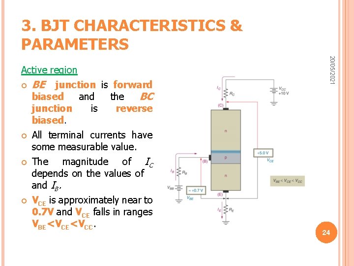
3. BJT CHARACTERISTICS & PARAMETERS BE junction is forward biased and the BC junction is reverse biased. All terminal currents have some measurable value. The magnitude of IC depends on the values of β and IB. VCE is approximately near to 0. 7 V and VCE falls in ranges VBE<VCC. 20/05/2021 Active region 24
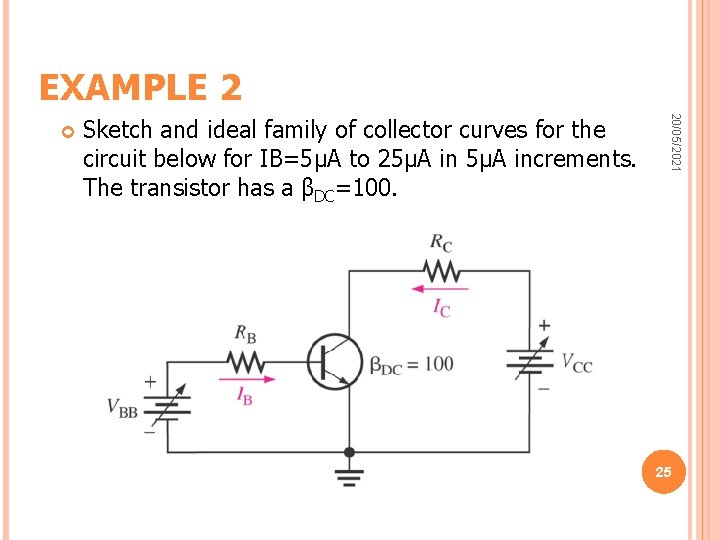
EXAMPLE 2 Sketch and ideal family of collector curves for the circuit below for IB=5μA to 25μA increments. The transistor has a βDC=100. 20/05/2021 25
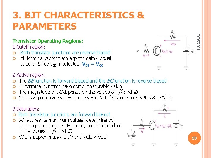
3. BJT CHARACTERISTICS & PARAMETERS 20/05/2021 Transistor Operating Regions: 1. Cutoff region: Both transistor junctions are reverse biased All terminal current are approximately equal to zero. Since ICEO neglected, VCE = VCC 2. Active region: The BE junction is forward biased and the BC junction is reverse biased All terminal currents have some measurable value The magnitude of IC depends on the values of and IB VCE is approximately near to 0. 7 V and VCE falls in ranges VBE<VCC 3. Saturation: Both transistor junctions are forward biased IC reaches its maximum values- determine by the component in the CE circuit, and independent of the values of and IB VBE is approximately 0. 7 V and VCE < VBE 26
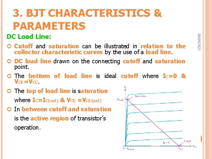
3. BJT CHARACTERISTICS & PARAMETERS Cutoff and saturation can be illustrated in relation to the collector characteristic curves by the use of a load line. 20/05/2021 DC Load Line: DC load line drawn on the connecting cutoff and saturation point. The bottom of load line is ideal cutoff where IC=0 & VCE=VCC. The top of load line is saturation where IC=IC(sat) & VCE =VCE(sat) In between cutoff and saturation is the active region of transistor’s operation. 27
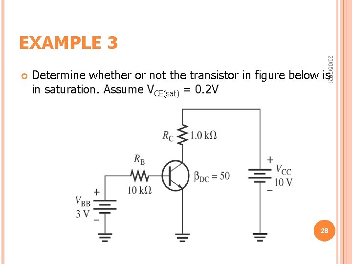
EXAMPLE 3 20/05/2021 Determine whether or not the transistor in figure below is in saturation. Assume VCE(sat) = 0. 2 V 28
20/05/2021 4. BJT AS AN AMPLIFIER 29
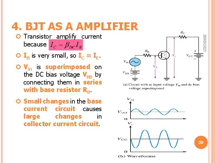
4. BJT AS A AMPLIFIER IB is very small, so IC ≈ IE. 20/05/2021 Transistor amplify current because Vin is superimposed on the DC bias voltage VBB by connecting them in series with base resistor RB. Small changes in the base current circuit causes large changes in collector current circuit. 30
20/05/2021 5. BJT AS A SWITCH 31
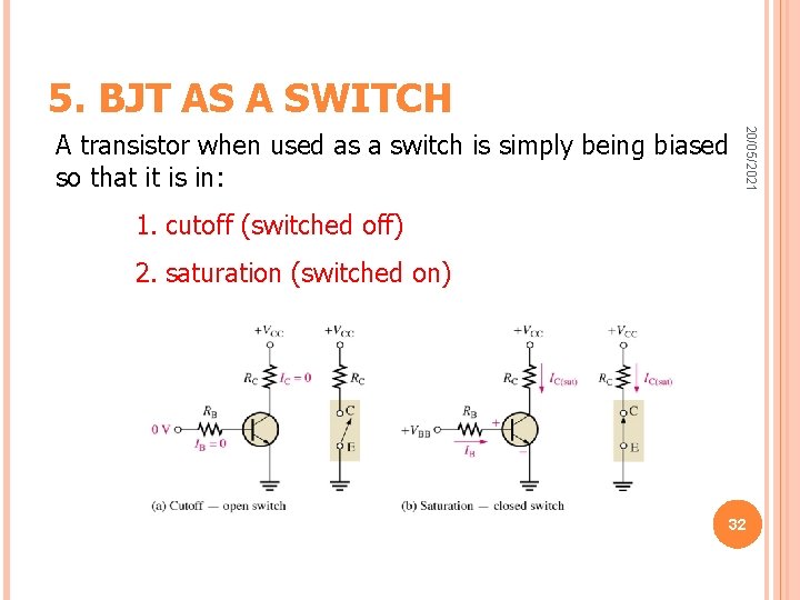
5. BJT AS A SWITCH 20/05/2021 A transistor when used as a switch is simply being biased so that it is in: 1. cutoff (switched off) 2. saturation (switched on) 32
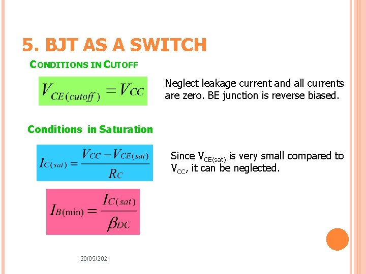
5. BJT AS A SWITCH CONDITIONS IN CUTOFF Neglect leakage current and all currents are zero. BE junction is reverse biased. Conditions in Saturation Since VCE(sat) is very small compared to VCC, it can be neglected. 20/05/2021 33
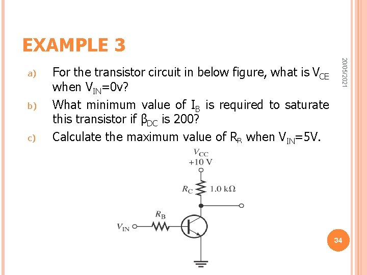
EXAMPLE 3 b) c) For the transistor circuit in below figure, what is VCE when VIN=0 v? What minimum value of IB is required to saturate this transistor if βDC is 200? Calculate the maximum value of RB when VIN=5 V. 20/05/2021 a) 34
20/05/2021 6. SUMMARY 35
6. SUMMARY 20/05/2021 The bipolar junction transistor (BJT) is constructed of three regions: base, collector, and emitter. The BJT has two p-n junctions, the base-emitter junction and the base-collector junction. The two types of transistors are pnp and npn. For the BJT to operate as an amplifier, the base-emitter junction is forward biased and the collector-base junction is reverse biased (transistor in active region). Of the three currents IB is very small in comparison to IE and IC. Beta is the current gain of a transistor. This the ratio of I C/IB. 36
6. SUMMARY When the transistor is off it is in cutoff condition (no current). 20/05/2021 A transistor can be operated as an electronics switch. When the transistor is on, it is in saturation condition (maximum current). Beta can vary with temperature and also varies from transistor to transistor. 37
- Slides: 37