1 Basic Semiconductor Physics Outline Material Issues Compound
1. Basic Semiconductor Physics • Outline: - Material Issues: - Compound Semiconductors? - Epitaxy, Lattice Matching and Strained Layers Physical Issues: - Energy Bands - Quantum-Size Effect - Light Generation and Recombination - Device Issues: - Design Rule of LD/LEDs - Ohmic Contacts
Material Issues: - Introduction to compound semiconductors (CS) - Basic energy band structures of CS - Hetero-junction structures (LM, Strained layers) - Epitaxial growth – MBE, MOCVD

1. 1 What is a “Semiconductor” ? • Criterion: by bandgap – Conductivity, Wavelength change A few impurity concentration changes Si into a good conductor. This variability of electrical properties makes semiconductors natural choices for electronic devices.
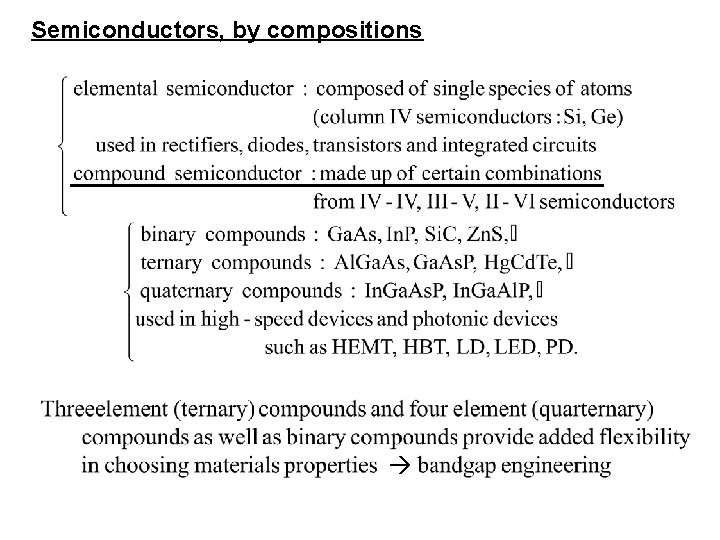
Semiconductors, by compositions
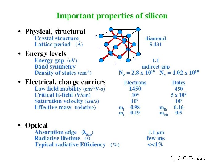
By C. G. Fonstad
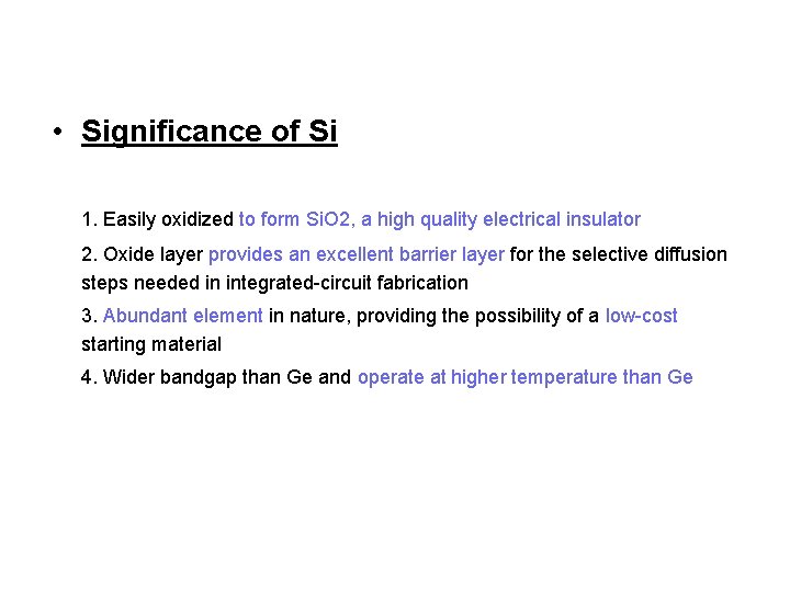
• Significance of Si 1. Easily oxidized to form Si. O 2, a high quality electrical insulator 2. Oxide layer provides an excellent barrier layer for the selective diffusion steps needed in integrated-circuit fabrication 3. Abundant element in nature, providing the possibility of a low-cost starting material 4. Wider bandgap than Ge and operate at higher temperature than Ge
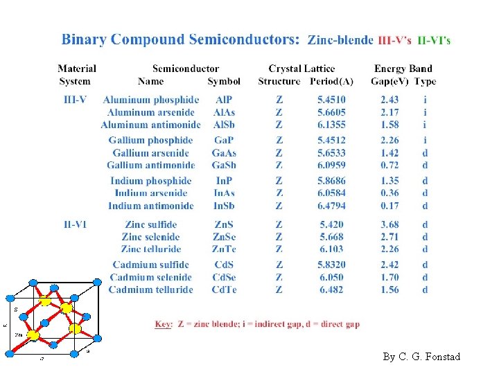
By C. G. Fonstad

Compound Semiconductors (examples) (i) binary compound semiconductors Si. C, Zn. Se, Ga. N → Blue LED/LD Ga. P, Ga. N Green ~ Yellow (for N doping) Red (for Zn & O doping) Ga. As, In. P, In. As → IR (ii) ternary compound semiconductors: Ga. Px. As 1 -x, Alx. Ga 1 -x. As, Gax. In 1 -x. As indirect Solid state electron devices, B. G. Streetman
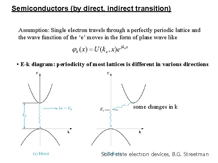
Semiconductors (by direct, indirect transition) Assumption: Single electron travels through a perfectly periodic lattice and the wave function of the ‘e’ moves in the form of plane wave like • E-k diagram: periodicity of most lattices is different in various directions some changes in k Solid state electron devices, B. G. Streetman
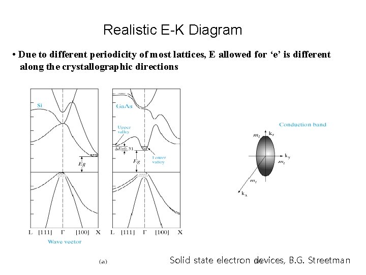
Realistic E-K Diagram • Due to different periodicity of most lattices, E allowed for ‘e’ is different along the crystallographic directions Solid state electron devices, B. G. Streetman
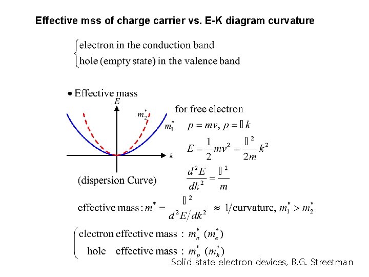
Effective mss of charge carrier vs. E-K diagram curvature Solid state electron devices, B. G. Streetman
Combination of Compound Semiconductors and The Properties of Strained Layers
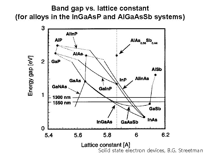
Band gap vs. lattice constant (for alloys in the In. Ga. As. P and Al. Ga. As. Sb systems) Solid state electron devices, B. G. Streetman
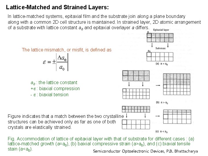
Lattice-Matched and Strained Layers: In lattice-matched systems, epitaxial film and the substrate join along a plane boundary along with a common 2 D cell structure is maintained. In strained layer, 2 D atomic arrangement of a substrate with lattice constant a 0 and epitaxial overlayer a differs. The lattice mismatch, or misfit, is defined as a 0 : the lattice constant + : biaxial compression - : biaxial tension Figure indicates that a match between the two crystalline structures can be achieved only as far as one of both crystals are elastically strained. Fig. Accommodation of lattice of epitaxial layer with that of substrate for different cases : (a) lattice-matched growth (a=a 0), (b) baixial compressive strain (a>a 0), and (c) biaxial tensile stain (a<a 0). Semiconductor Optoelectronic Devices, P. B. Bhattacharya
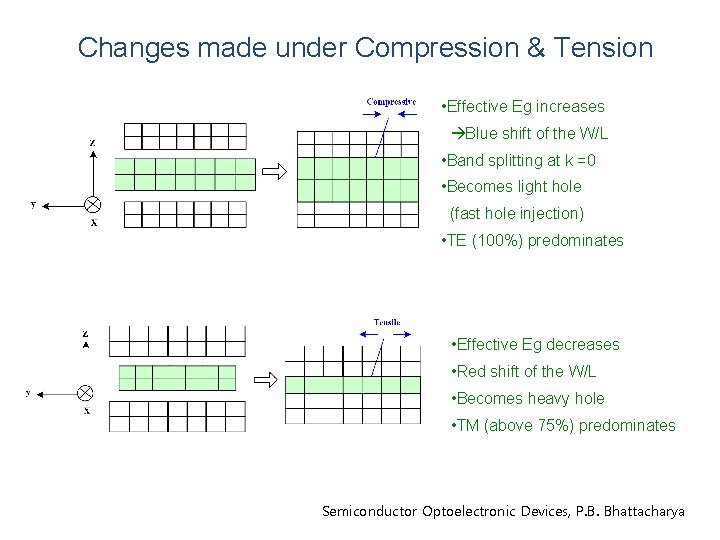
Changes made under Compression & Tension • Effective Eg increases Blue shift of the W/L • Band splitting at k =0 • Becomes light hole (fast hole injection) • TE (100%) predominates • Effective Eg decreases • Red shift of the W/L • Becomes heavy hole • TM (above 75%) predominates Semiconductor Optoelectronic Devices, P. B. Bhattacharya
- Slides: 15