1 5 Ground planes and layer stacking 2


- Slides: 19

1 5. Ground planes and layer stacking 전자파 연구실

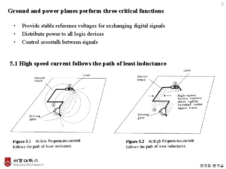
2 Ground and power planes perform three critical functions • • • Provide stable reference voltages for exchanging digital signals Distribute power to all logic devices Control crosstalk between signals 5. 1 High speed current follows the path of least inductance 전자파 연구실

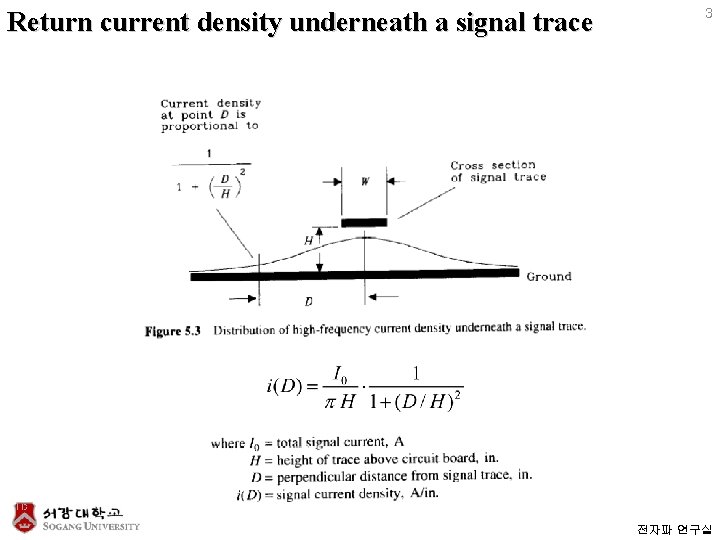
Return current density underneath a signal trace 3 전자파 연구실

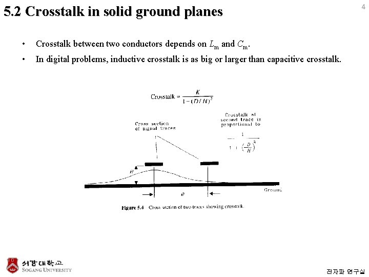
5. 2 Crosstalk in solid ground planes 4 • Crosstalk between two conductors depends on Lm and Cm. • In digital problems, inductive crosstalk is as big or larger than capacitive crosstalk. 전자파 연구실

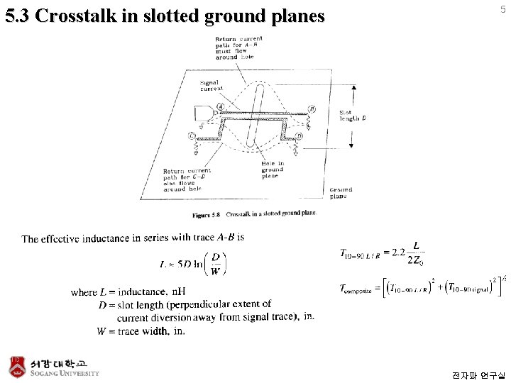
5. 3 Crosstalk in slotted ground planes 5 전자파 연구실

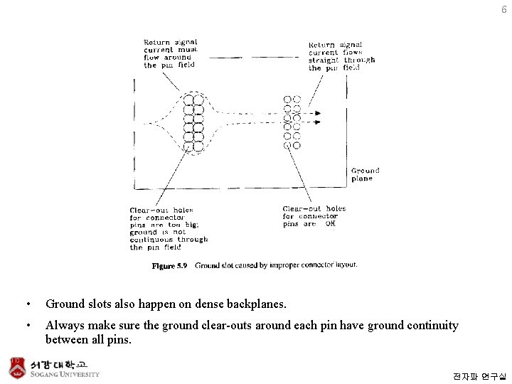
6 • Ground slots also happen on dense backplanes. • Always make sure the ground clear-outs around each pin have ground continuity between all pins. 전자파 연구실

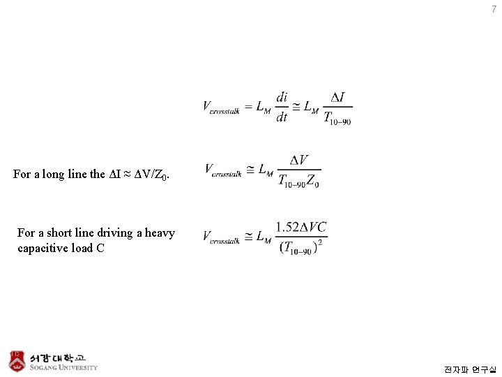
7 For a long line the ΔI ≈ ΔV/Z 0. For a short line driving a heavy capacitive load C 전자파 연구실

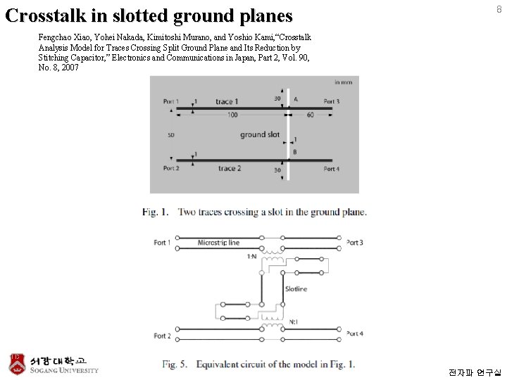
Crosstalk in slotted ground planes 8 Fengchao Xiao, Yohei Nakada, Kimitoshi Murano, and Yoshio Kami, “Crosstalk Analysis Model for Traces Crossing Split Ground Plane and Its Reduction by Stitching Capacitor, ” Electronics and Communications in Japan, Part 2, Vol. 90, No. 8, 2007 전자파 연구실

Crosstalk reduction using stitching capacitors 9 전자파 연구실

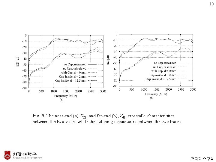
10 Fig. 9. The near-end (a), S 21, and far-end (b), S 41, crosstalk characteristics between the two traces while the stitching capacitor is between the two traces. 전자파 연구실

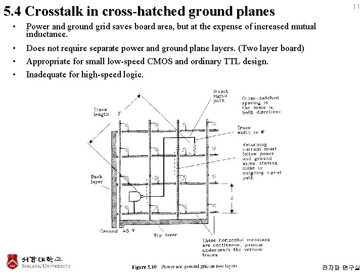
5. 4 Crosstalk in cross-hatched ground planes • Power and ground grid saves board area, but at the expense of increased mutual inductance. • • • Does not require separate power and ground plane layers. (Two layer board) Appropriate for small low-speed CMOS and ordinary TTL design. Inadequate for high-speed logic. 11 전자파 연구실

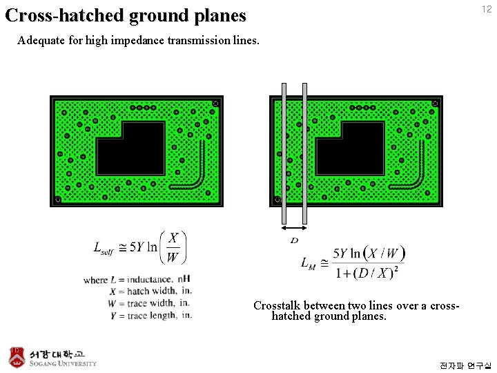
Cross-hatched ground planes 12 Adequate for high impedance transmission lines. Crosstalk between two lines over a crosshatched ground planes. 전자파 연구실

5. 5 Crosstalk with power and ground fingers 13 Don’t use this. Massive amount of self and mutual inductance is introduced. 전자파 연구실

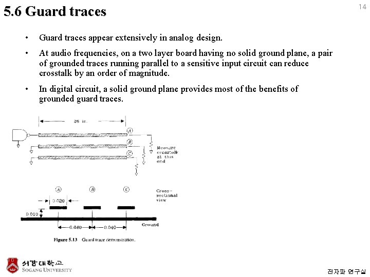
5. 6 Guard traces 14 • Guard traces appear extensively in analog design. • At audio frequencies, on a two layer board having no solid ground plane, a pair of grounded traces running parallel to a sensitive input circuit can reduce crosstalk by an order of magnitude. • In digital circuit, a solid ground plane provides most of the benefits of grounded guard traces. 전자파 연구실

5. 8 How to stack printed circuit board layers 15 5. 8. 1 Power and ground planning • Specify signal rise time, number of the signals, physical dimensions of the board • Make a guess as to the track width. • Estimate self and mutual inductance using solid, hatched, and power-ground fingers. • If you use a solid ground plane, plan on using ground and power planes in pairs to prevent warping in the circuit board. 전자파 연구실

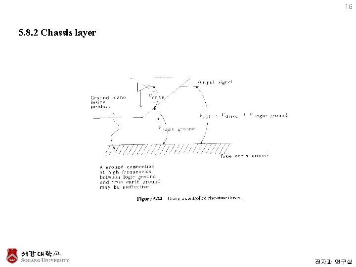
16 5. 8. 2 Chassis layer 전자파 연구실

17 5. 8. 3 Selecting trace dimensions • High density signal line decrease PCB cost. • High density traces increase crosstalk, increase power handling capacity. • Minimum trace width is limited by production processes. 5. 8. 4 Routing density vs. number of routing layers 전자파 연구실

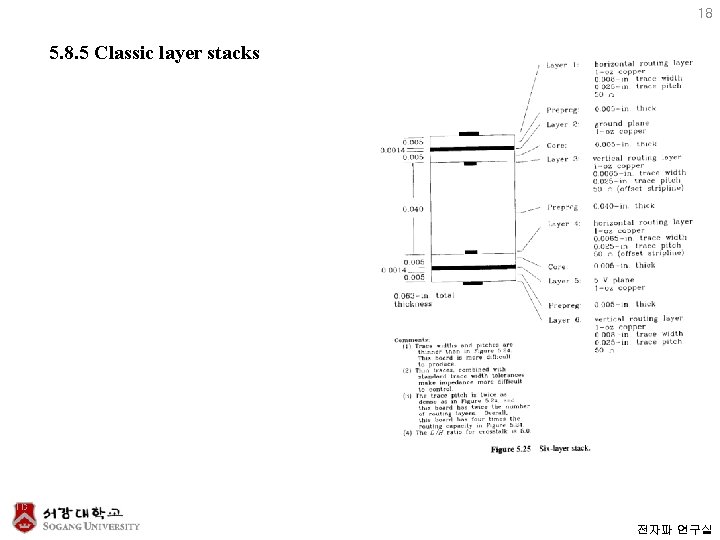
18 5. 8. 5 Classic layer stacks 전자파 연구실
