1 2 1 Latches FlipFlops and Registers Figure
- Slides: 28

1

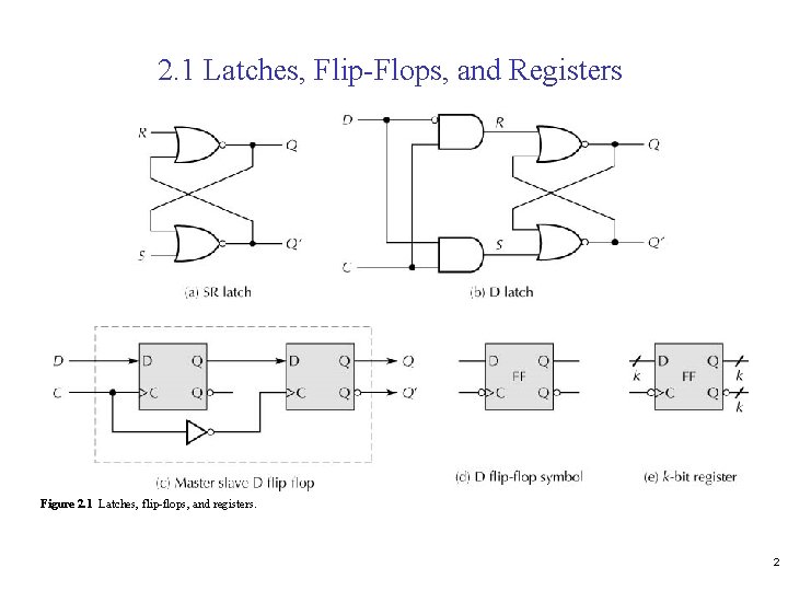
2. 1 Latches, Flip-Flops, and Registers Figure 2. 1 Latches, flip-flops, and registers. 2

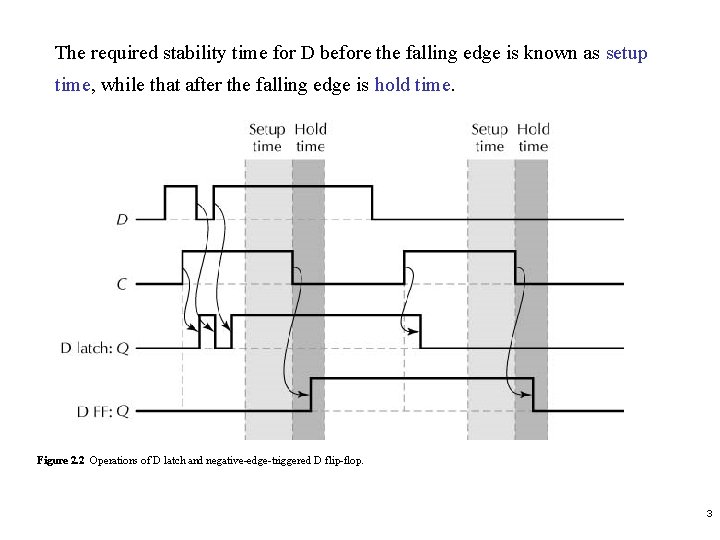
The required stability time for D before the falling edge is known as setup time, while that after the falling edge is hold time. Figure 2. 2 Operations of D latch and negative-edge-triggered D flip-flop. 3

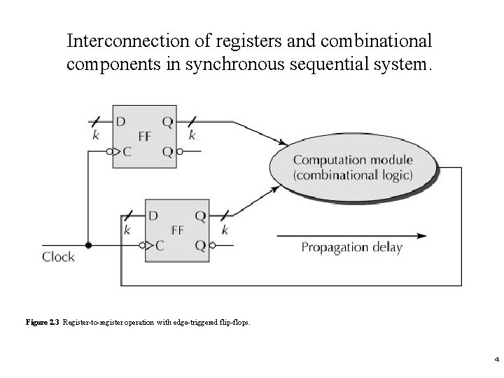
Interconnection of registers and combinational components in synchronous sequential system. Figure 2. 3 Register-to-register operation with edge-triggered flip-flops. 4

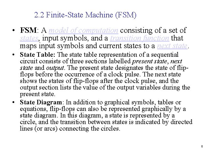
2. 2 Finite-State Machine (FSM) • FSM: A model of computation consisting of a set of states, input symbols, and a transition function that maps input symbols and current states to a next state. • State Table: The state table representation of a sequential circuit consists of three sections labelled present state, next state and output. The present state designates the state of flipflops before the occurrence of a clock pulse. The next state shows the states of flip-flops after the clock pulse, and the output section lists the value of the output variables during the present state. • State Diagram: In addition to graphical symbols, tables or equations, flip-flops can also be represented graphically by a state diagram. In this diagram, a state is represented by a circle, and the transition between states is indicated by directed lines (or arcs) connecting the circles. 5

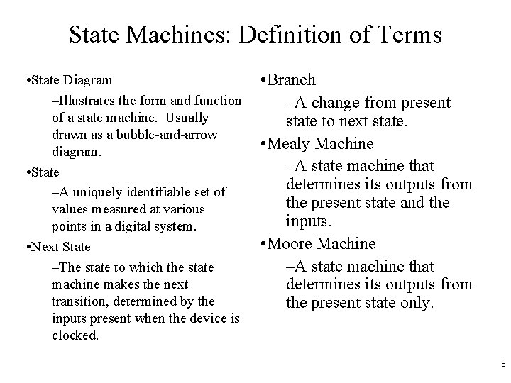
State Machines: Definition of Terms • State Diagram –Illustrates the form and function of a state machine. Usually drawn as a bubble-and-arrow diagram. • State –A uniquely identifiable set of values measured at various points in a digital system. • Next State –The state to which the state machine makes the next transition, determined by the inputs present when the device is clocked. • Branch –A change from present state to next state. • Mealy Machine –A state machine that determines its outputs from the present state and the inputs. • Moore Machine –A state machine that determines its outputs from the present state only. 6

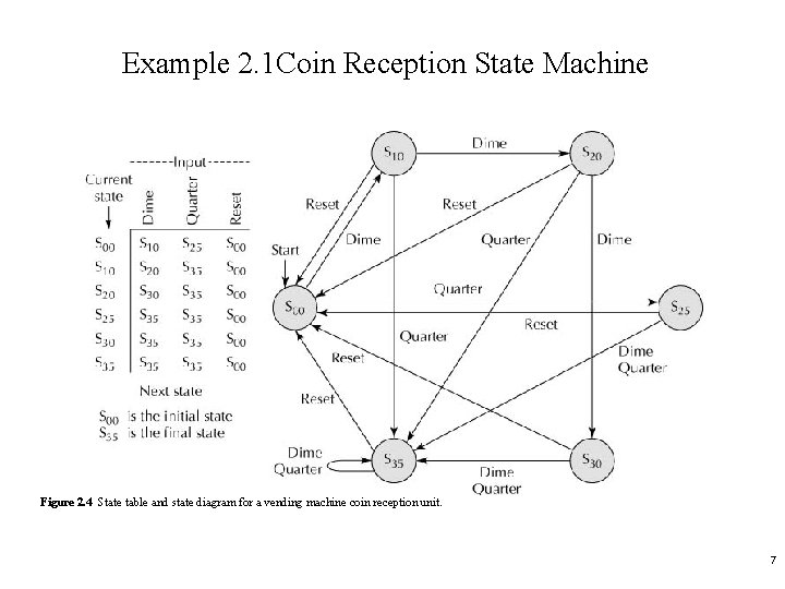
Example 2. 1 Coin Reception State Machine Figure 2. 4 State table and state diagram for a vending machine coin reception unit. 7

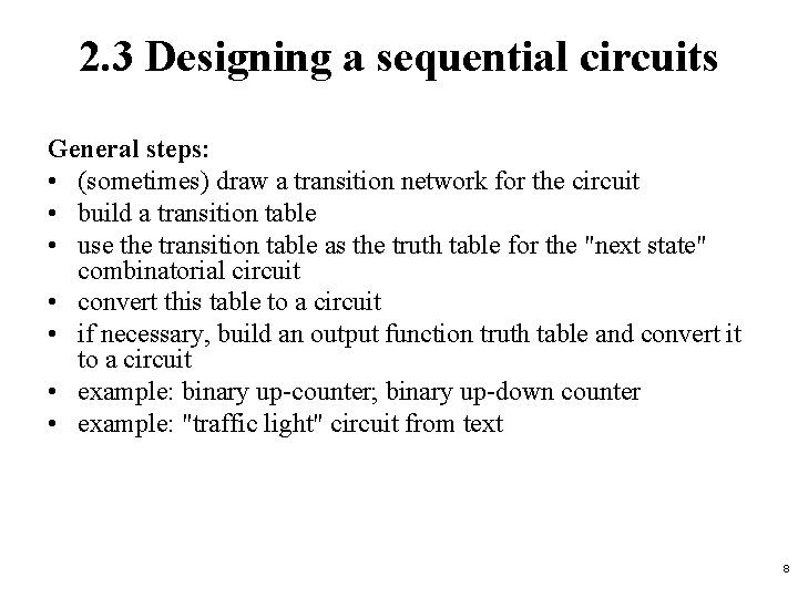
2. 3 Designing a sequential circuits General steps: • (sometimes) draw a transition network for the circuit • build a transition table • use the transition table as the truth table for the "next state" combinatorial circuit • convert this table to a circuit • if necessary, build an output function truth table and convert it to a circuit • example: binary up-counter; binary up-down counter • example: "traffic light" circuit from text 8

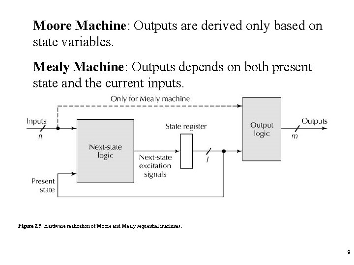
Moore Machine: Outputs are derived only based on state variables. Mealy Machine: Outputs depends on both present state and the current inputs. Figure 2. 5 Hardware realization of Moore and Mealy sequential machines. 9

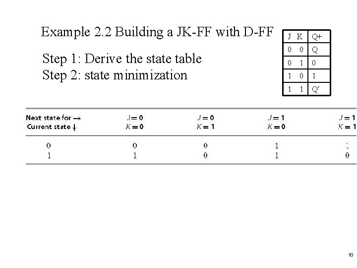
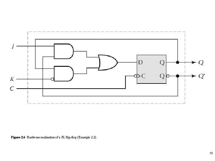
Example 2. 2 Building a JK-FF with D-FF Step 1: Derive the state table Step 2: state minimization J K Q+ 0 0 Q 0 1 0 1 1 1 Q’ 10

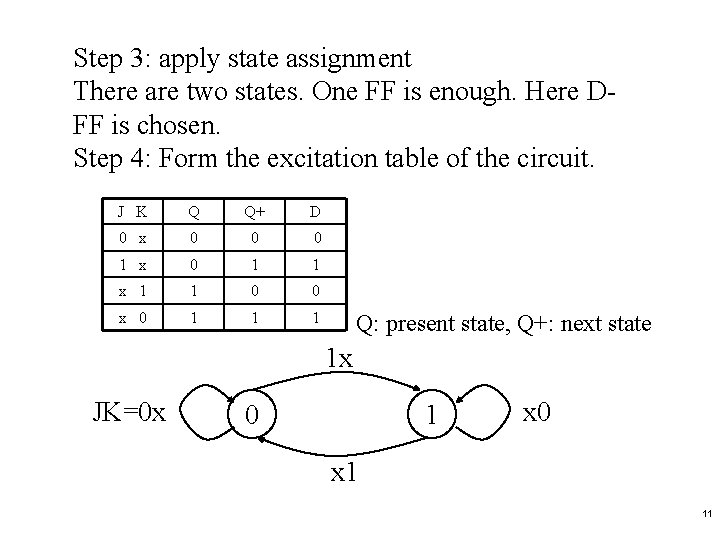
Step 3: apply state assignment There are two states. One FF is enough. Here DFF is chosen. Step 4: Form the excitation table of the circuit. J K Q Q+ D 0 x 0 0 0 1 x 0 1 1 x 1 1 0 0 x 0 1 1 1 Q: present state, Q+: next state 1 x JK=0 x 0 1 x 0 x 1 11

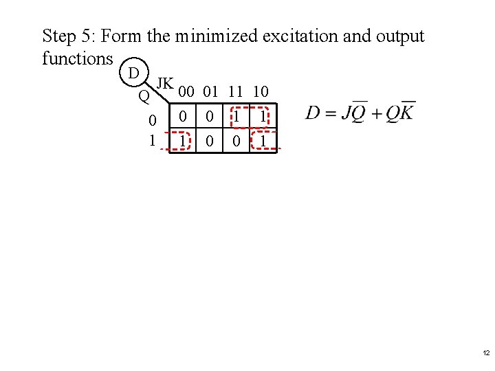
Step 5: Form the minimized excitation and output functions D JK 00 01 11 10 Q 0 0 0 1 12

Figure 2. 6 Hardware realization of a JK flip-flop (Example 2. 2). 13

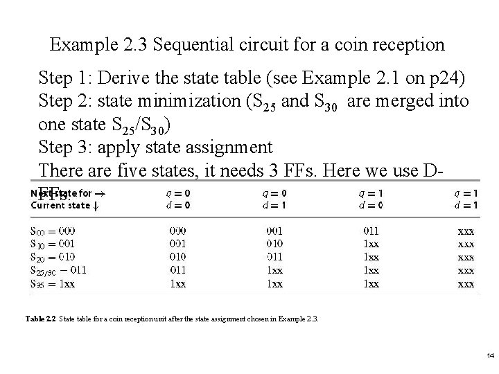
Example 2. 3 Sequential circuit for a coin reception Step 1: Derive the state table (see Example 2. 1 on p 24) Step 2: state minimization (S 25 and S 30 are merged into one state S 25/S 30) Step 3: apply state assignment There are five states, it needs 3 FFs. Here we use DFFs. Table 2. 2 State table for a coin reception unit after the state assignment chosen in Example 2. 3. 14

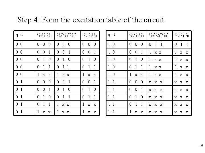
Step 4: Form the excitation table of the circuit q d Q 2 Q 1 Q 0 Q 2+Q 1+Q 0+ D 2 D 1 D 0 0 0 0 1 0 0 0 1 1 0 0 1 1 0 0 0 1 1 x x 0 0 0 1 0 1 x x 0 0 0 1 1 1 0 0 1 1 1 x x 0 0 1 x x 1 0 1 x x 0 1 0 0 1 1 1 0 0 0 x x x 0 1 0 1 1 0 0 1 x x x 0 1 0 0 1 1 1 1 0 x x x 0 1 1 1 x x 1 1 0 1 1 x x x 0 1 1 x x 1 1 1 x x x x 15

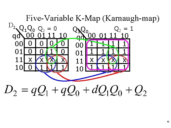
Five-Variable K-Map (Karnaugh-map) D 2 Q Q 1 0 qd 00 00 0 01 0 11 x 10 0 Q 1 Q 0 01 11 10 qd 00 0 00 1 0 01 1 x x x 11 x 1 10 1 Q 2 = 0 Q 2 = 1 01 11 1 1 x x 1 1 10 1 1 x 1 16

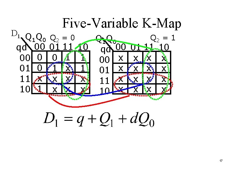
D 1 Q Q 1 0 qd 00 00 0 01 0 11 x 10 1 Five-Variable K-Map Q 1 Q 0 01 11 10 qd 00 0 1 1 00 x 1 01 x x x x 10 x Q 2 = 0 Q 2 = 1 01 11 x x x x 10 x x 17

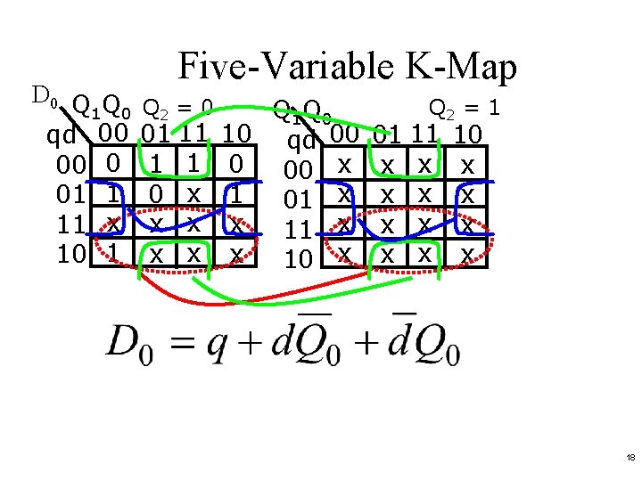
D 0 Q Q 1 0 qd 00 00 0 01 1 11 x 10 1 Five-Variable K-Map Q 1 Q 0 01 11 10 qd 00 1 1 0 00 x 1 01 x x x x 10 x Q 2 = 0 Q 2 = 1 01 11 x x x x 10 x x 18

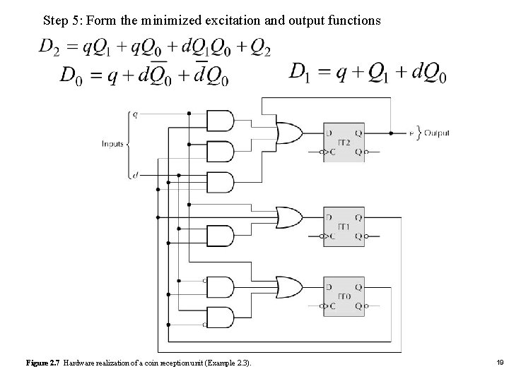
Step 5: Form the minimized excitation and output functions Figure 2. 7 Hardware realization of a coin reception unit (Example 2. 3). 19

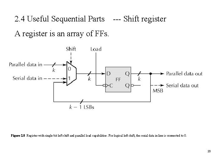
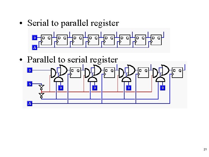
2. 4 Useful Sequential Parts --- Shift register A register is an array of FFs. Figure 2. 8 Register with single-bit left shift and parallel load capabilities. For logical left shift, the serial data in line is connected to 0. 20

• Serial to parallel register • Parallel to serial register 21

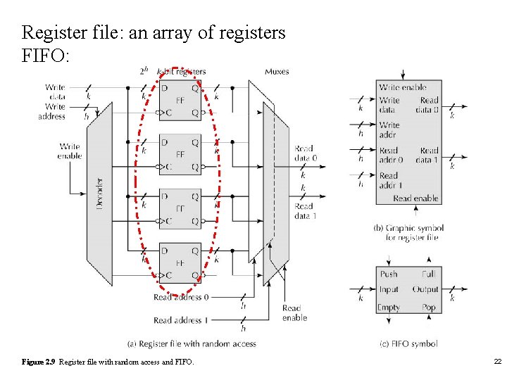
Register file: an array of registers FIFO: Figure 2. 9 Register file with random access and FIFO. 22

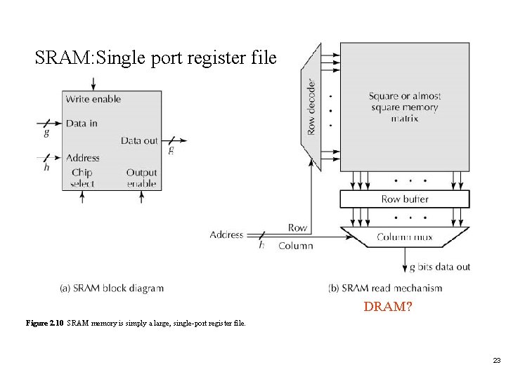
SRAM: Single port register file DRAM? Figure 2. 10 SRAM memory is simply a large, single-port register file. 23

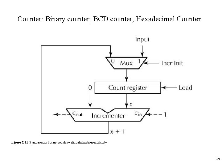
Counter: Binary counter, BCD counter, Hexadecimal Counter Figure 2. 11 Synchronous binary counter with initialization capability. 24

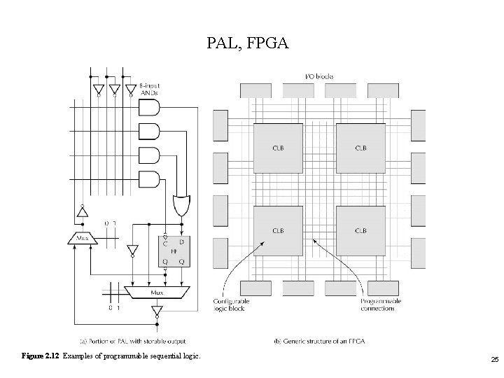
PAL, FPGA Figure 2. 12 Examples of programmable sequential logic. 25

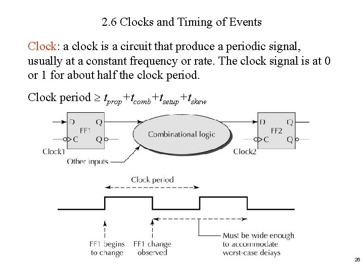
2. 6 Clocks and Timing of Events Clock: a clock is a circuit that produce a periodic signal, usually at a constant frequency or rate. The clock signal is at 0 or 1 for about half the clock period. Clock period tprop+tcomb+tsetup+tskew 26

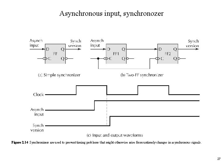
Asynchronous input, synchronozer Figure 2. 14 Synchronizers are used to prevent timing problems that might otherwise arise from untimely changes in asynchronous signals. 27

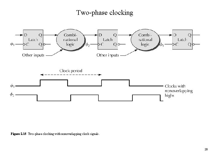
Two-phase clocking Figure 2. 15 Two-phase clocking with nonoverlapping clock signals. 28