06 0725 ICPS Tu A 3 o 3
- Slides: 13

’ 06 07/25 ICPS Tu. A 3 o. 3 Tue 17: 30 Poster Band-edge divergence and Fermi-edge singularity in an n-type doped T-shaped quantum wire T. Ihara 1, M. Yoshita 1, H. Akiyama 1, L. N. Pfeiffer 2 and K. W. West 2 1 Institute for Solid State Physics, University of Tokyo and CREST, JST, Chiba 2778581, Japan 2 Bell Laboratories, Lucent Technologies, Murray Hill, NJ 07974, USA

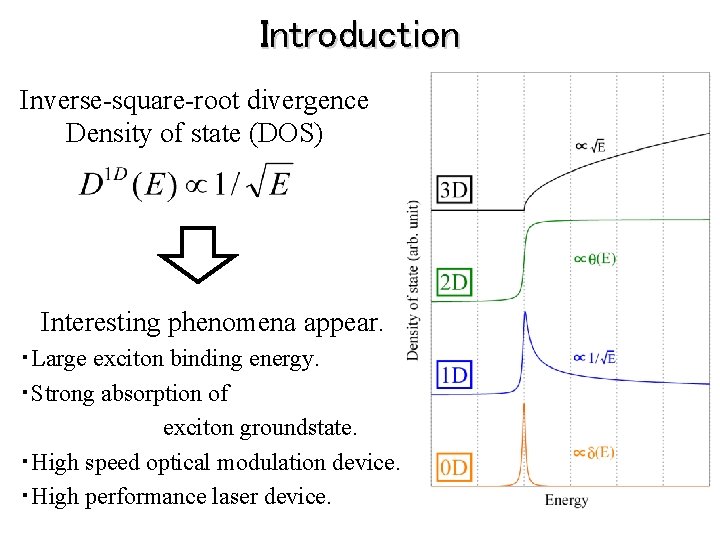
Introduction Inverse-square-root divergence Density of state (DOS) Interesting phenomena appear. ・Large exciton binding energy. ・Strong absorption of exciton groundstate. ・High speed optical modulation device. ・High performance laser device.

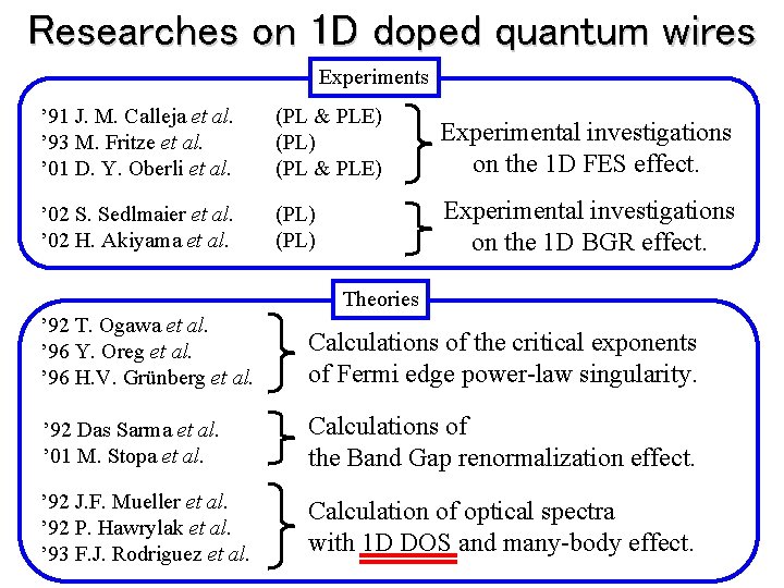
Researches on 1 D doped quantum wires Experiments ’ 91 J. M. Calleja et al. ’ 93 M. Fritze et al. ’ 01 D. Y. Oberli et al. (PL & PLE) Experimental investigations on the 1 D FES effect. ’ 02 S. Sedlmaier et al. ’ 02 H. Akiyama et al. (PL) Experimental investigations on the 1 D BGR effect. Theories ’ 92 T. Ogawa et al. ’ 96 Y. Oreg et al. ’ 96 H. V. Grünberg et al. Calculations of the critical exponents of Fermi edge power-law singularity. ’ 92 Das Sarma et al. ’ 01 M. Stopa et al. Calculations of the Band Gap renormalization effect. ’ 92 J. F. Mueller et al. ’ 92 P. Hawrylak et al. ’ 93 F. J. Rodriguez et al. Calculation of optical spectra with 1 D DOS and many-body effect.

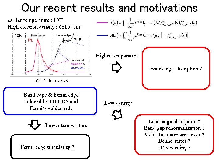
Our recent results and motivations carrier temperature : 10 K High electron density : 6 x 105 cm-1 Higher temperature Band-edge absorption ? ’ 04 T. Ihara et. al. Band edge & Fermi edge induced by 1 D DOS and Fermi’s golden rule Lower temperature Fermi edge singularity ? Low density Band-edge absorption ? Band gap renormalization ? Metal-Insulator crossover ? Bound states ? 1 D screening ?

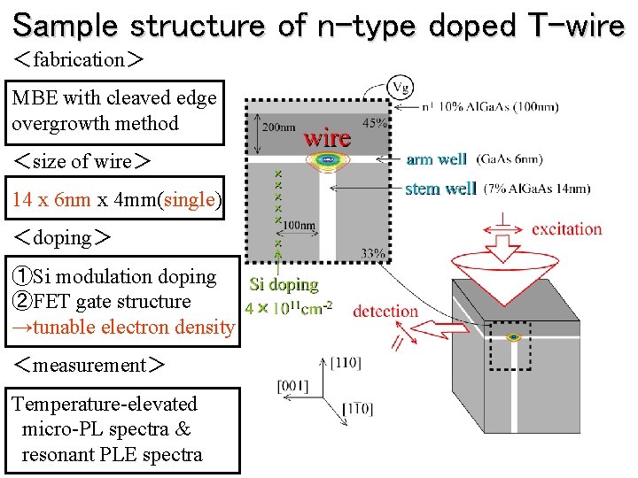
Sample structure of n-type doped T-wire <fabrication> MBE with cleaved edge overgrowth method <size of wire> 14 x 6 nm x 4 mm(single) <doping> ①Si modulation doping ②FET gate structure →tunable electron density <measurement> Temperature-elevated micro-PL spectra & resonant PLE spectra

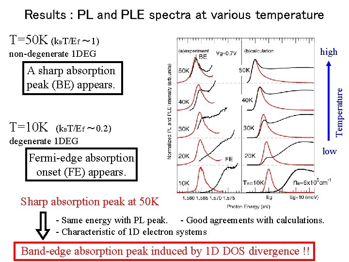
Results : PL and PLE spectra at various temperature T=50 K (k T/Ef ~ 1) B non-degenerate 1 DEG high Temperature A sharp absorption peak (BE) appears. T=10 K (k. BT/Ef ~ 0. 2) degenerate 1 DEG Fermi-edge absorption onset (FE) appears. low Sharp absorption peak at 50 K - Same energy with PL peak. - Good agreements with calculations. - Characteristic of 1 D electron systems Band-edge absorption peak induced by 1 D DOS divergence !!

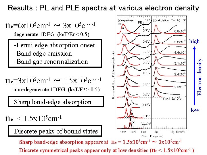
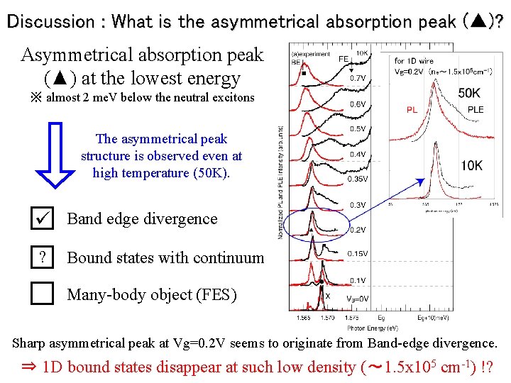
Results : PL and PLE spectra at various electron density ne=6 x 105 cm-1 ~ 3 x 105 cm-1 degenerate 1 DEG (k. BT/Ef < 0. 5) Electron density -Fermi edge absorption onset -Band edge emission -Band gap renormalization high ne=3 x 105 cm-1 ~ 1. 5 x 105 cm-1 non-degenerate 1 DEG (k. BT/Ef > 0. 5) Sharp band-edge absorption ne low < 1. 5 x 105 cm-1 Discrete peaks of bound states Sharp band-edge absorption appears at ne = 1. 5 x 105 cm-1 ~ 3 x 105 cm-1 Discrete symmetrical peaks appear only at low densities (ne < 1. 5 x 105 cm-1 )

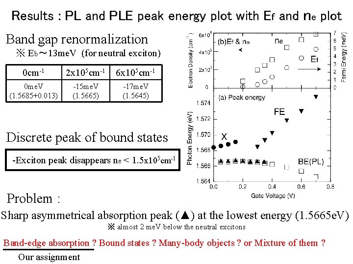
Results : PL and PLE peak energy plot with Ef and ne plot Band gap renormalization ※ Eb~ 13 me. V (for neutral exciton) 0 cm-1 0 me. V (1. 5685+0. 013) 2 x 105 cm-1 6 x 105 cm-1 -15 me. V (1. 5665) -17 me. V (1. 5645) Discrete peak of bound states -Exciton peak disappears ne < 1. 5 x 105 cm-1 Problem : Sharp asymmetrical absorption peak (▲) at the lowest energy (1. 5665 e. V) ※ almost 2 me. V below the neutral excitons Band-edge absorption ? Bound states ? Many-body objects ? or Mixture of them ? Our assignment

Discussion : What is the asymmetrical absorption peak (▲)? Asymmetrical absorption peak (▲) at the lowest energy ※ almost 2 me. V below the neutral excitons The asymmetrical peak structure is observed even at high temperature (50 K). ü Band edge divergence ? Bound states with continuum Many-body object (FES) Sharp asymmetrical peak at Vg=0. 2 V seems to originate from Band-edge divergence. ⇒ 1 D bound states disappear at such low density (~ 1. 5 x 105 cm-1) !?

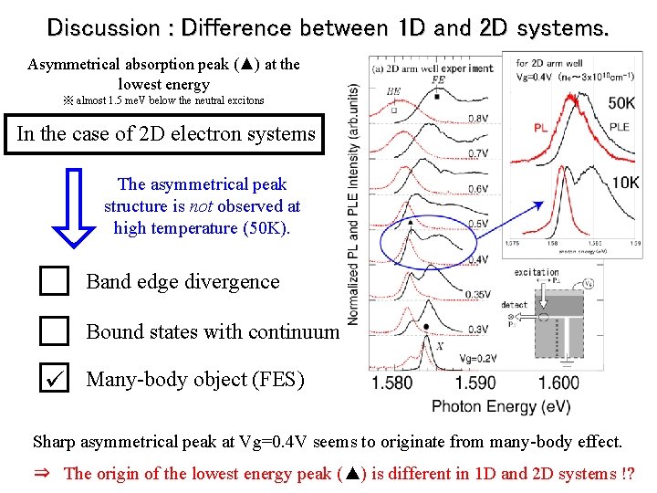
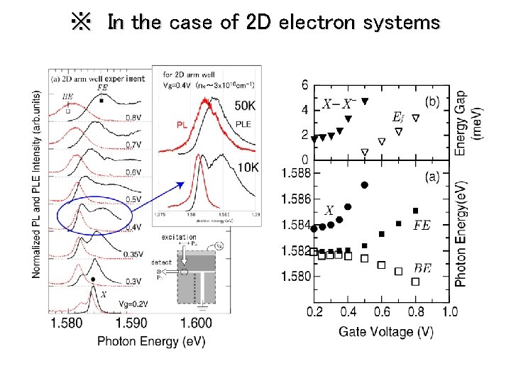
Discussion : Difference between 1 D and 2 D systems. Asymmetrical absorption peak (▲) at the lowest energy ※ almost 1. 5 me. V below the neutral excitons In the case of 2 D electron systems The asymmetrical peak structure is not observed at high temperature (50 K). Band edge divergence Bound states with continuum ü Many-body object (FES) Sharp asymmetrical peak at Vg=0. 4 V seems to originate from many-body effect. ⇒ The origin of the lowest energy peak (▲) is different in 1 D and 2 D systems !?

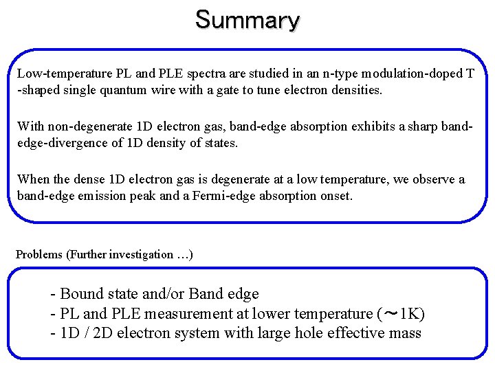
Summary Low-temperature PL and PLE spectra are studied in an n-type modulation-doped T -shaped single quantum wire with a gate to tune electron densities. With non-degenerate 1 D electron gas, band-edge absorption exhibits a sharp bandedge-divergence of 1 D density of states. When the dense 1 D electron gas is degenerate at a low temperature, we observe a band-edge emission peak and a Fermi-edge absorption onset. Problems (Further investigation …) - Bound state and/or Band edge - PL and PLE measurement at lower temperature (~ 1 K) - 1 D / 2 D electron system with large hole effective mass

※ In the case of 2 D electron systems

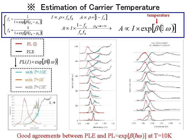
※ Estimation of Carrier Temperature temperature PL (I) PLE with T=10 K with T=5 K with T=15 K Good agreements between PLE and PL×exp[β(ћω)] at T=10 K