0 35 m CMOS NMOS StarHSpiceCMOSNNMOS Spice MODEL
. MODEL CMOSN NMOS (LEVEL = 49")
(续) +RDSW = 1. 88264 E 3 +WR")
(续) +UC 1 = -5. 6 E-11 +WLN")

 • Constant Voltage理论(CV) • Quasi-Constant Voltage理论(QCV)")


- Slides: 25
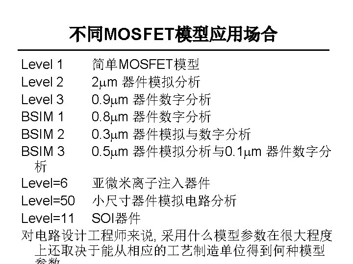
台积电公司某一批 0. 35 m CMOS 艺NMOS器件 的Star-HSpice参数(命名为CMOSN的NMOS模型 库Spice文件). MODEL CMOSN NMOS (LEVEL = 49 +VERSION = 3. 1 TNOM= 27 TOX = 7. 6 E-9 +XJ = 1 E-7 NCH = 2. 3579 E 17 VTH 0 = 0. 5085347 +K 1 = 0. 5435268 K 2 = 0. 0166934 K 3 = 2. 745303 E-3 +K 3 B = 0. 6056312 W 0 = 1 E-7 NLX = 2. 869371 E-7 +DVT 0 W =0 DVT 1 W =0 DVT 2 W =0 +DVT 0 = 1. 7544494 DVT 1 = 0. 4703288 DVT 2 = -0. 0394498 +U 0 = 489. 0696189 UA = 5. 339423 E-10 UB = 1. 548022 E-18 +UC = 5. 795283 E-11 VSAT = 1. 191395 E 5 A 0 = 0. 8842702 +AGS = 0. 1613116 B 0 = 1. 77474 E-6 B 1 = 5 E-6 +KETA= 5. 806511 E-3 A 1 =0 A 2 =1
台积电公司某一批 0. 35 m CMOS 艺NMOS器件的Star. HSpice参数(命名为CMOSN的NMOS模型库Spice文件)(续) +RDSW = 1. 88264 E 3 +WR =1 +XL = -2 E-8 +DWB = 9. 792339 E-9 +CIT =0 +CDSCB = 0 +DSUB = 0. 2068625 +PDIBLC 2 = 5. 597608 E-3 +PSCBE 1 = 4. 863898 E 8 +DELTA = 0. 01 +UTE = -1. 5 +KT 2 = 0. 022 PRWG = -0. 105799 WINT = 7. 381398 E-8 XW =0 VOFF = -0. 0951708 CDSC = 4. 922742 E-3 ETA 0 = 2. 005052 E-3 PCLM = 1. 9418893 PDIBLCB = -4. 18062 E-4 PSCBE 2 = 1. 70429 E-5 MOBMOD = 1 KT 1 = -0. 11 UA 1 = 4. 31 E-9 PRWB = -0. 0152046 LINT = 1. 030561 E-8 DWG = -1. 493222 E-8 NFACTOR = 1. 2401249 CDSCD = 0 ETAB = 5. 106831 E-3 PDIBLC 1 = 0. 2403315 DROUT = 0. 5527689 PVAG = 1. 0433116 PRT =0 KT 1 L =0 UB 1 = -7. 61 E-18
台积电公司某一批 0. 35 m CMOS 艺NMOS器件的Star. HSpice参数(命名为CMOSN的NMOS模型库Spice文件)(续) +UC 1 = -5. 6 E-11 +WLN =1 +WWL =0 +LW =0 +CAPMOD= 2 +CGSO = 1. 96 E-10 +PB = 0. 7644361 +PBSW = 0. 8683237 +PRDSW = -159. 9288563 +LKETA = -6. 965933 E-3 +ELM =5 *END CMOSN AT WW LL LWN XPART CGBO MJ MJSW PK 2 PAGS ) = 3. 3 E 4 = -1. 22182 E-15 =0 =1 = 0. 4 =0 = 0. 3394296 = 0. 1808065 = -9. 424037 E-4 = 0. 0718 WL WWN LLN LWL CGDO CJ CJSW PVTH 0 WKETA NQSMOD =0 = 1. 137 =1 =0 = 1. 96 E-10 = 9. 384895 E-4 = 2. 885151 E-10 = -0. 0101318 = 4. 696914 E-3 =1
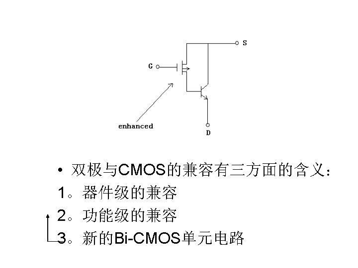
CMOS device
Theory • Constant Electric Field理论(CE) • Constant Voltage理论(CV) • Quasi-Constant Voltage理论(QCV)
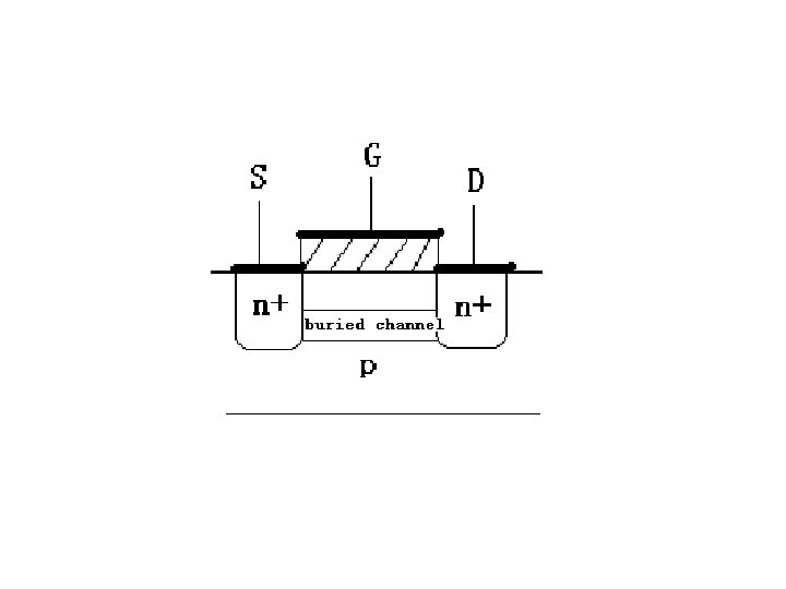
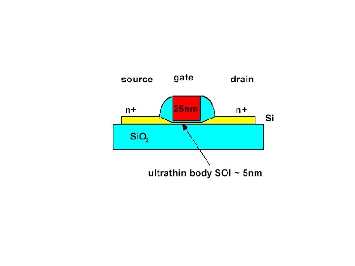
• Figure: Cross-sectional view of a self-aligned poly-silicon gate transistor with LOCOS isolation
LDD As the channel length becomes smaller, the junction electric fields become larger. One approach that reduces these breakdown effects is to alter the doping profile of the drain contact. Peak electric field changes.
As indicated by the ITRS roadmap scaling of conventional bulk CMOS transistors is becoming more and more difficult for the 45 nm technology node and beyond. This is because very high doping concentrations in the channel and ultra shallow junctions are needed in the channel in order to suppress short channel effects. Another critical issue is that probably high k dielectrics will be needed with an equivalent oxide thickness below 1 nm necessary to achieve the desired on currents in the range of 1 m. A/µm at power supply voltages below 1 V. Although several transistors with extremely short channels have been demonstrated in the literature, they all suffer from lack of performance. Therefore, novel transistor concepts for CMOS are under investigation.
Fin. FET